
Solid-state image capturing apparatus, driving method thereof and electronic apparatus

a technology of solid-state image and driving method, which is applied in the direction of television system, television system scanning details, radioation control devices, etc., can solve the problem achieve the effect of reducing layout efficiency or sensitivity

Active Publication Date: 2010-07-29
SONY CORP
View PDF5 Cites 30 Cited by
  • Summary
  • Abstract
  • Description
  • Claims
  • Application Information

AI Technical Summary

Benefits of technology

[0009]However, if a configuration, in which the charge discharging transistor is newly added to the pixel, is employed, since the number of signal interconnections for driving the charge discharging transistor is increased, layout efficiency is reduced. Further, since the number of interconnections of interconnection layers of an upper layer of the photoelectric conversion unit as the increase in the number of the signal interconnections, if light incident to the photoelectric conversion unit is rejected by upper layer interconnections, the amount of light incident into the photoelectric conversion unit is reduced, so that sensitivity is reduced.
[0010]In view of the above issues, it is desirable to provide a solid-state image capturing apparatus, which can prevent layout efficiency and sensitivity from being reduced even in the case of employing a pixel structure having a charge discharging transistor, a driving method thereof, and an electronic apparatus having the same.
[0013]According to the invention, in the pixel structure provided with the charge discharging transistor, the charge discharging transistor can be driven even without adding a dedicated signal line, so that reduction in the layout efficiency or sensitivity accompanied by the addition of the charge discharging transistor is not caused.

Problems solved by technology

However, if a configuration, in which the charge discharging transistor is newly added to the pixel, is employed, since the number of signal interconnections for driving the charge discharging transistor is increased, layout efficiency is reduced.

Method used


Image

  • Solid-state image capturing apparatus, driving method thereof and electronic apparatus
  • Solid-state image capturing apparatus, driving method thereof and electronic apparatus
  • Solid-state image capturing apparatus, driving method thereof and electronic apparatus

Examples


first embodiment

2. First Embodiment

[System Configuration]

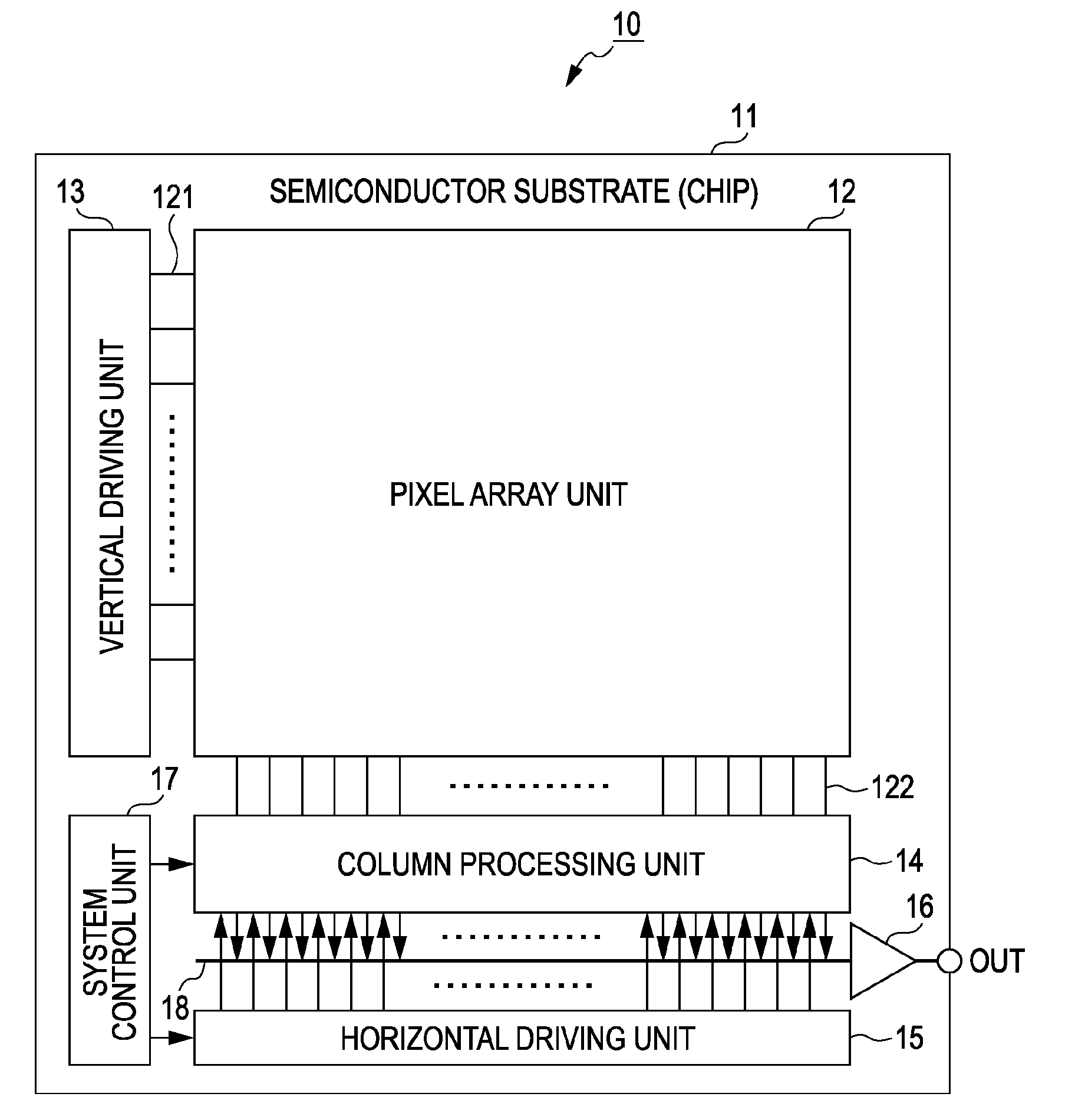
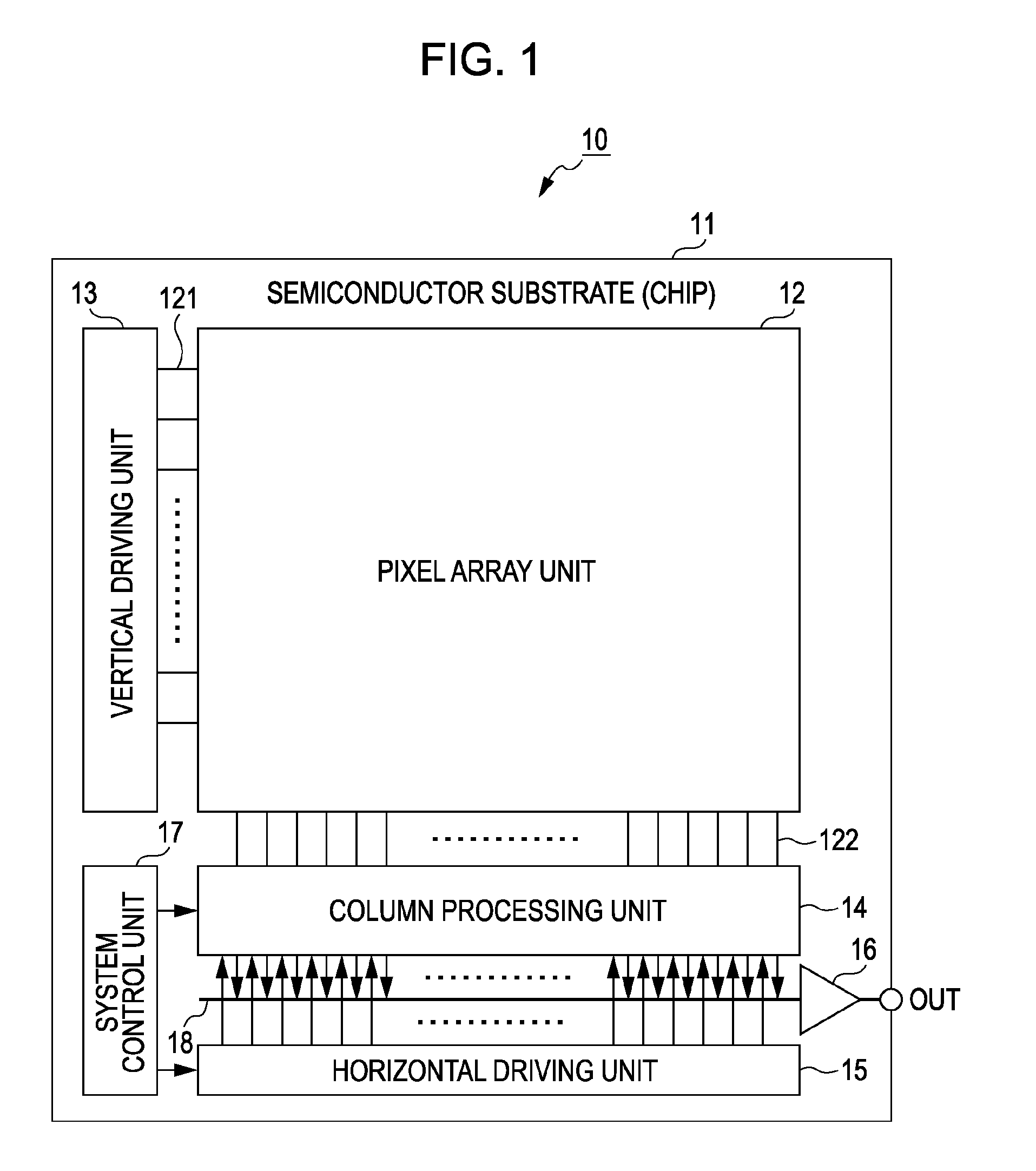
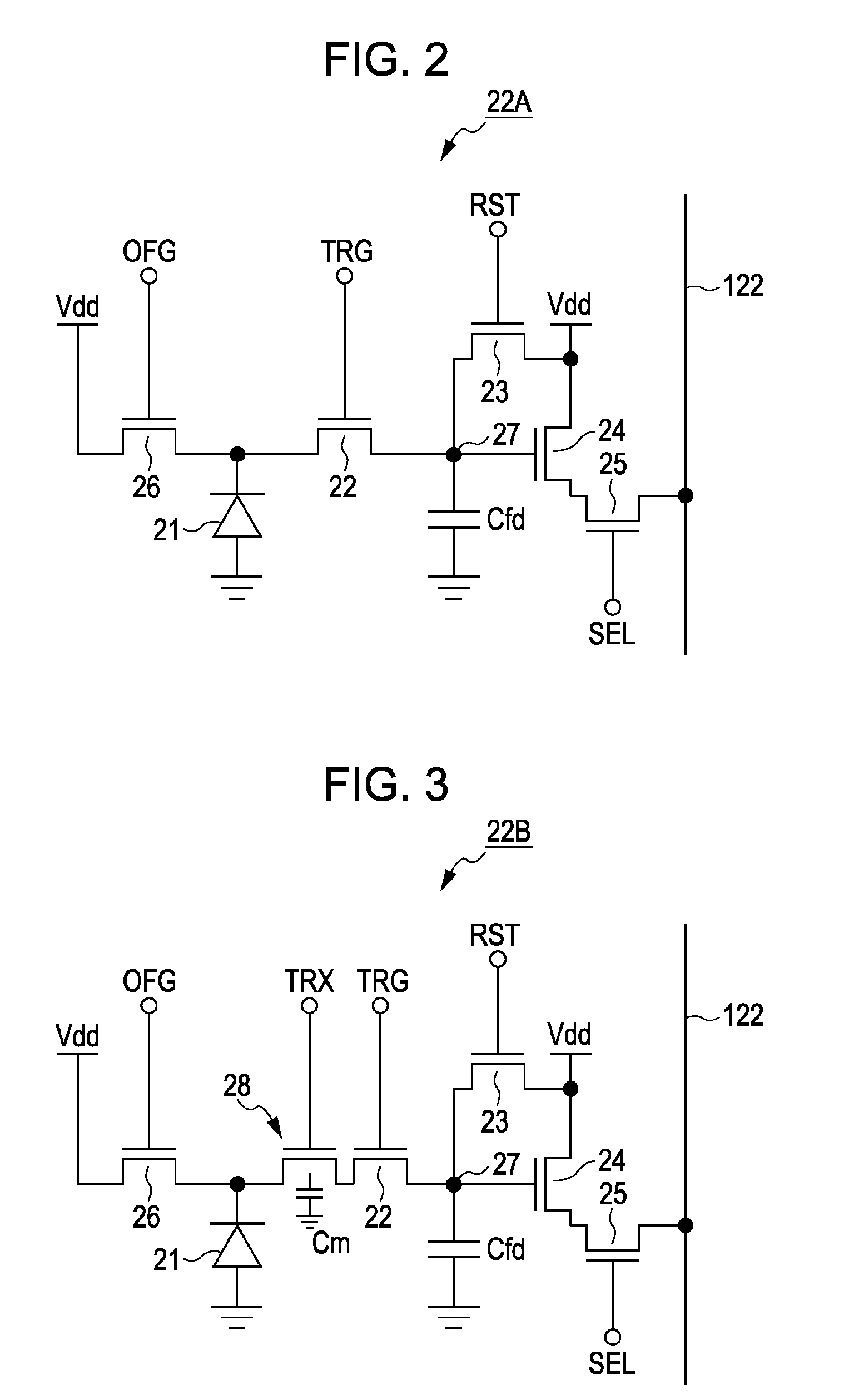
[0079]FIG. 4 is a circuit diagram illustrating the configuration of main elements of the CMOS image sensor according to the first embodiment of the invention. Herein, the CMOS image sensor, in which the unit pixel 20A of the circuit example 1 shown in FIG. 2 is two-dimensionally arranged, is described as an example. Further, in order to simplify FIG. 4, two unit pixels 20A-i and 20A-i−1 of a certain pixel column, which are vertically adjacent to each other, are representatively shown.

[0080]As shown in FIG. 4, in the unit pixels 20A-i and 20A-i−1, as the pixel driving lines 121, for example, three driving lines such as a transmission line 121-1, a reset line 121-2 and a selection line 121-3 are provided to each pixel row. These driving lines 121-1, 121-2 and 121-3 are respectively connected to output terminals corresponding to the vertical driving unit 13 by each pixel row.

[0081]Then, description will be given while focusing on an ith pixel ro...

second embodiment

3. Second Embodiment

[0100]FIG. 8 is a circuit diagram illustrating the configuration of main elements of the CMOS image sensor according to the second embodiment of the invention. In FIG. 8, the same reference numerals are used to designate the same elements as those shown in FIG. 4.

[0101]The CMOS image sensor according to the embodiment is based on the CMOS image sensor in which the unit pixel 20A of the circuit example 1 shown in FIG. 2 is two-dimensionally arranged. Further, in order to simplify FIG. 8, two unit pixels 20A-i and 20A-i−1 of a certain pixel column, which are vertically adjacent to each other, are representatively shown.

[0102]As shown in FIG. 8, in the unit pixels 20A-i and 20A-i−1, as the pixel driving lines 121, for example, three driving lines such as the transmission line 121-1, the reset line 121-2 and the selection line 121-3 are provided by each pixel row. These driving lines 121-1, 121-2 and 121-3 are respectively connected to output terminals corresponding ...

third embodiment

4. Third Embodiment

[System Configuration]

[0108]FIG. 9 is a circuit diagram illustrating the configuration of main elements of the CMOS image sensor according to the third embodiment of the invention. In FIG. 9, the same reference numerals are used to designate the same elements as those shown in FIG. 4.

[0109]The CMOS image sensor according to the embodiment is based on the CMOS image sensor in which the unit pixel of the circuit example 2 shown in FIG. 3, that is, the unit pixel 20B including the memory unit 28 that holds charges inside the pixel is two-dimensionally arranged. Further, in order to simplify FIG. 9, two unit pixels 20B-i and 20B-i−1 of a certain pixel column, which are vertically adjacent to each other, are representatively shown.

[0110]As shown in FIG. 9, in the unit pixels 20B-i and 20B-i−1, as the pixel driving lines 121, for example, four driving lines such as the transmission line 121-1, the reset line 121-2, the selection line 121-3 and the transmission line 121-...


PUM


Abstract

A solid-state image capturing apparatus includes: a pixel array unit including two-dimensionally arranged pixels each including a photoelectric conversion unit, a transfer transistor that transfers charges accumulated in the photoelectric conversion unit, and a charge discharging transistor that selectively discharges the charges accumulated in the photoelectric conversion unit; and a driving unit that performs driving for reading signals from each pixel of the pixel array unit, and drives the charge discharging transistor by using a signal for the driving.

Description

BACKGROUND OF THE INVENTION[0001]1. Technical Field[0002]The present invention relates to a solid-state image capturing apparatus, a driving method thereof and an electronic apparatus. In particular, the invention relates to a solid-state image capturing apparatus, such as a CMOS image sensor, having an electronic shutter function, a driving method thereof, and an electronic apparatus having the same.[0003]2. Description of the Related Art[0004]Most CMOS image sensors, which are a kind of a solid-state image capturing apparatus, for example, an X-Y address type solid-state image capturing apparatus, have an electronic shutter function for electronically performing an operation of resetting signal charges accumulated in photoelectric converters (light receiving units) and newly starting accumulation of signal charges. In general, a CMOS image sensor employs a so-called rolling shutter (also referred to as a focal plane shutter) scheme for performing the starting and ending of exposur...

Claims


Application Information

Patent Timeline
Patent Type & Authority Applications(United States)
IPC IPC(8): H04N5/335H04N25/00H01L27/146
CPCH01L27/14609H04N5/3741H04N5/3745H04N5/378H04N5/37452H04N5/37457H04N5/374H04N25/766H04N25/778H04N25/771H04N25/77H04N25/76H04N25/532H04N25/78H04N25/75
Inventor OIKE, YUSUKE
Owner SONY CORP
Learn More