Display Device and Method for Manufacturing Thereof
a technology for display devices and manufacturing methods, applied in the manufacture of electrode systems, electric discharge tubes/lamps, instruments, etc., can solve the problems of limitation in the fabrication of slim display devices having a small size, and achieve the effects of small size, coupling force, and slim structur
- Summary
- Abstract
- Description
- Claims
- Application Information
AI Technical Summary
Benefits of technology
Problems solved by technology
Method used
Image
Examples
first embodiment
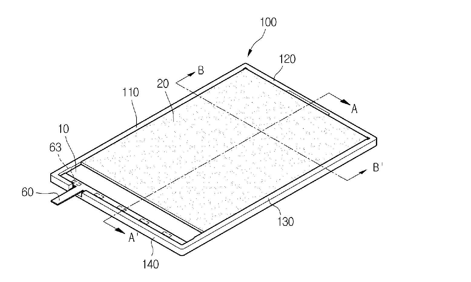
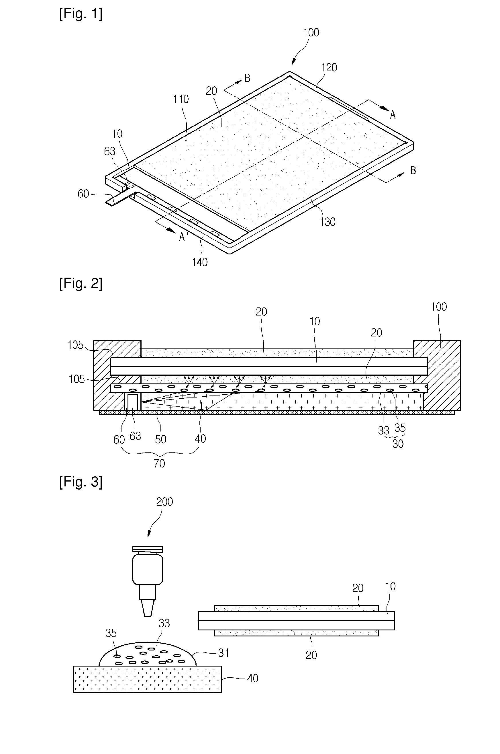
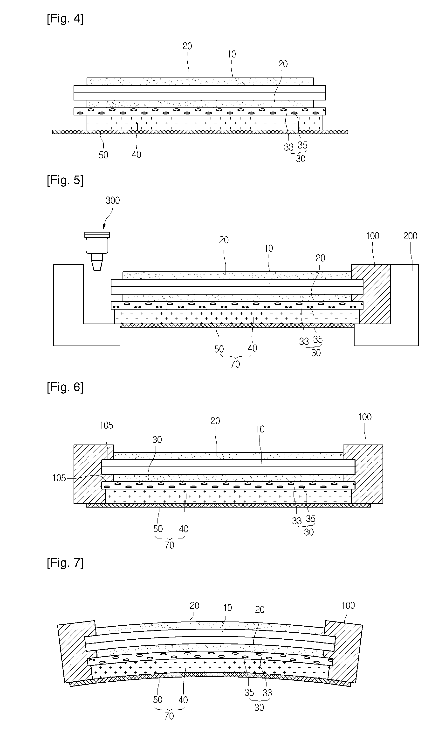
[0028]FIG. 1 is a perspective view showing a display device and FIG. 2 is a sectional view taken along line A-A in FIG. 1.
[0029]Referring to FIGS. 1 to 2, the display device according to the first embodiment comprises a liquid crystal panel 10, a backlight unit 70, an adhesive sheet 30 for light diffusion, and a frame 100.
[0030]The liquid crystal panel 10 is formed by interposing a liquid crystal layer between a TFT substrate and a color filter substrate. Further, a polarizer film 20 is formed on the upper and lower portions of the liquid crystal panel 10.
[0031]The backlight unit 70 comprises a light emitting section 60, a light guide plate 40 and a reflective sheet 50.
[0032]The light emitting section 60 comprises an LED (light emitting diode) 63, a CCFL (cold cathode fluorescent lamp) and the like, and outputs generated light to the light guide plate 40.
[0033]The light guide plate 40 receives the light generated from the light emitting section 60 to uniformly distribute the light ...
second embodiment
[0080]FIG. 8 is a sectional view showing a display device FIG. 9 is a sectional view showing the construction of a polarizer film coupled between the liquid crystal panel and the light guide plate shown in FIG. 8, and FIG. 10 is a sectional view showing a state in which the frame in FIG. 8 is bent.
[0081]Referring to in FIG. 8, the display device comprises the liquid crystal panel 10 and the backlight unit 70 as shown in FIG. 1.
[0082]The liquid crystal panel 10 is formed by interposing a liquid crystal layer between a TFT substrate and a color filter substrate. Further, first and second polarizer films 500 and 550 are formed on the upper and lower portions of the liquid crystal panel 10.
[0083]Since the backlight unit 70 has the same construction as that of the backlight unit of the first embodiment, detailed description thereof will be omitted. The backlight unit 70 comprises a light guide plate 40 and a reflective sheet 50. Further, an adhesive sheet for light diffusion may also be...
PUM
 Abstract
Description
Claims
Application Information
 - R&D Engineer
- R&D Manager
- IP Professional
- Industry Leading Data Capabilities
- Powerful AI technology
- Patent DNA Extraction
Browse by: Latest US Patents, China's latest patents, Technical Efficacy Thesaurus, Application Domain, Technology Topic, Popular Technical Reports.
© 2024 PatSnap. All rights reserved.Legal|Privacy policy|Modern Slavery Act Transparency Statement|Sitemap|About US| Contact US: help@patsnap.com


