Plasma CVD apparatus, method for forming thin film and semiconductor device
a technology of plasma cvd and thin film, applied in the direction of plasma technique, basic electric elements, coatings, etc., can solve the problems of failure to maintain the dielectric constant and mechanical strength, insufficient insulating properties, etc., and achieve high mechanical strength, stably maintained, and high mechanical strength
- Summary
- Abstract
- Description
- Claims
- Application Information
AI Technical Summary
Benefits of technology
Problems solved by technology
Method used
Image
Examples
embodiment 1
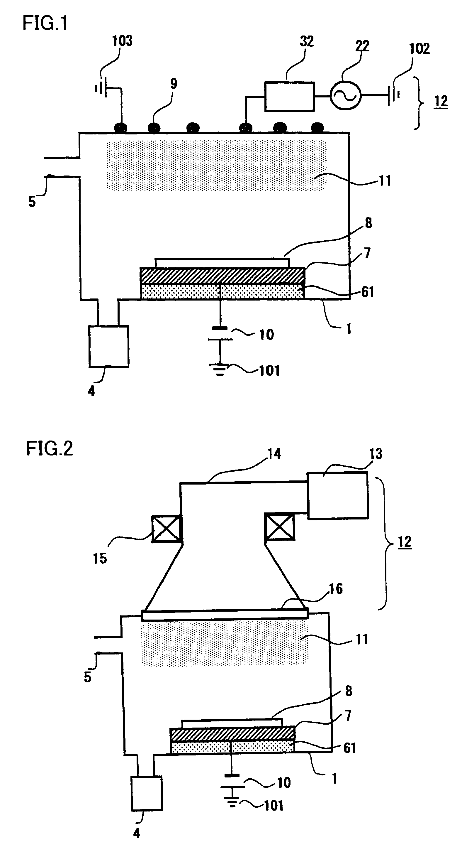
[0017]FIG. 1 is a schematic view that shows a schematic structure of a plasma CVD apparatus (hereinafter, referred to as a PCVD apparatus) in accordance with Embodiment 1 of the present invention. As shown in FIG. 1, the PCVD apparatus in accordance with the present invention is provided with a reaction chamber having a vacuum pump 4 and a material inlet 5 used for supplying a compound having a borazine skeleton, a feeding electrode 7 that is installed in reaction chamber 1 to support a substrate 8, and that is applied with a negative charge, and a plasma generator 12 that is arranged opposite to feeding electrode 7 via substrate 8 so as to generate a plasma 11 within reaction chamber 1.
[0018]In the PCVD apparatus of the present invention, a compound having a borazine skeleton is introduced into reaction chamber 1, with a plasma being generated within reaction chamber 1 by plasma generator 12 placed opposite to feeding electrode 7, so that the compound is excited, and by further app...
embodiment 2
[0034]The following description will discuss a film-forming process in which the PCVD apparatus in accordance with Embodiment 1 is used. First, substrate 8 is placed on feeding electrode 7, and the inside of reaction chamber 1 is vacuum-drawn. Next, a material gas (a compound having a borazine skeleton), a carrier gas and other gases, if necessary, are supplied into reaction chamber 1 through gas inlet 5. Moreover, the pressure inside reaction chamber 1 is vacuum-drawn by vacuum pump 4 to be maintained at a predetermined process pressure. Here, substrate 8 is set to a predetermined process temperature by using heating device 61 or heating / cooling device 62.
[0035]Moreover, when a high frequency is generated by high frequency power supply 22 so that plasma 11 is generated inside reaction chamber 1, the material gas (composition having a borazine skeleton) and the carrier gas are formed into ions and radicals in reaction chamber 1. Of these, the ions are drawn by the electrode having a...
embodiment 3
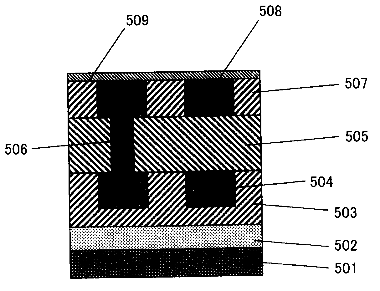
[0041]By using the PCVD apparatus shown in the above-mentioned Embodiment 1, a film formed by the thin-film forming method shown in the above-mentioned Embodiment 2 was used as an insulating layer and a wiring pattern made of copper was formed thereon, and these processes were repeated so that a semiconductor device having several laminated layers was manufactured. FIG. 5 is a schematic cross-sectional view showing one example of the semiconductor device. Insulating films 502 and 509, a first insulating layer 503, a second insulating layer 505 and a third insulating layer 507 were formed by using the PCVD apparatus shown in the above-mentioned Embodiment 1 through the thin-film forming method in accordance with the above-mentioned Embodiment 2. In the above-mentioned semiconductor device, it was confirmed that wiring delay could be reduced in comparison with the structure in which the insulating layers were made from silicon oxide or silicon nitride. Moreover, it was also confirmed ...
PUM
| Property | Measurement | Unit |
|---|---|---|
| temperature | aaaaa | aaaaa |
| dielectric constant | aaaaa | aaaaa |
| voltage | aaaaa | aaaaa |
Abstract
Description
Claims
Application Information
 - R&D
- Intellectual Property
- Life Sciences
- Materials
- Tech Scout
- Unparalleled Data Quality
- Higher Quality Content
- 60% Fewer Hallucinations
Browse by: Latest US Patents, China's latest patents, Technical Efficacy Thesaurus, Application Domain, Technology Topic, Popular Technical Reports.
© 2025 PatSnap. All rights reserved.Legal|Privacy policy|Modern Slavery Act Transparency Statement|Sitemap|About US| Contact US: help@patsnap.com


