
Radiation detecting system

a detection system and radiation detection technology, applied in radiation measurement, instruments, measurement devices, etc., can solve the problems of large difference in thermal expansion coefficient between carrier selective semi-insulating layers, large noise generation, image defect generation, etc., to suppress crystallization and reduce dark current without deteriorating sensitivity

Active Publication Date: 2010-07-01
FUJIFILM CORP
View PDF3 Cites 1 Cited by
  • Summary
  • Abstract
  • Description
  • Claims
  • Application Information

AI Technical Summary

Benefits of technology

[0010]In view of the foregoing observations and description, the primary object of the present invention is to provide a radiation detecting system which can give rectifying characteristics to the interface of the voltage imparting electrode and the photoconductive layer and reduce the dark current without deteriorating the sensitivity and at the same time, can suppress crystallization when a-Se is used as the photoconductive layer thereby overcoming a problem of peeling off of the carrier selective semi-insulating layer and the cracks in the carrier selective semi-insulating layer.
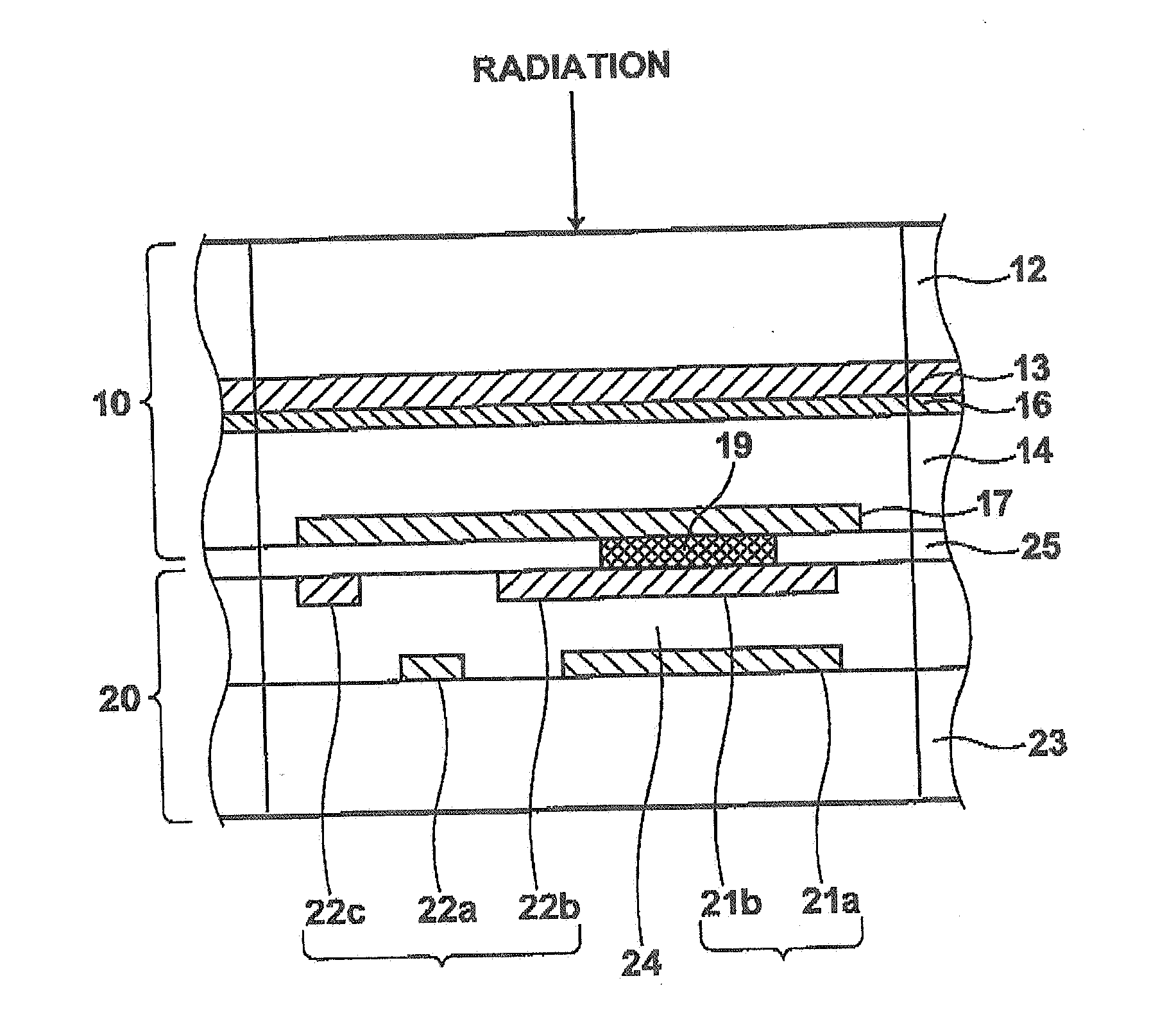
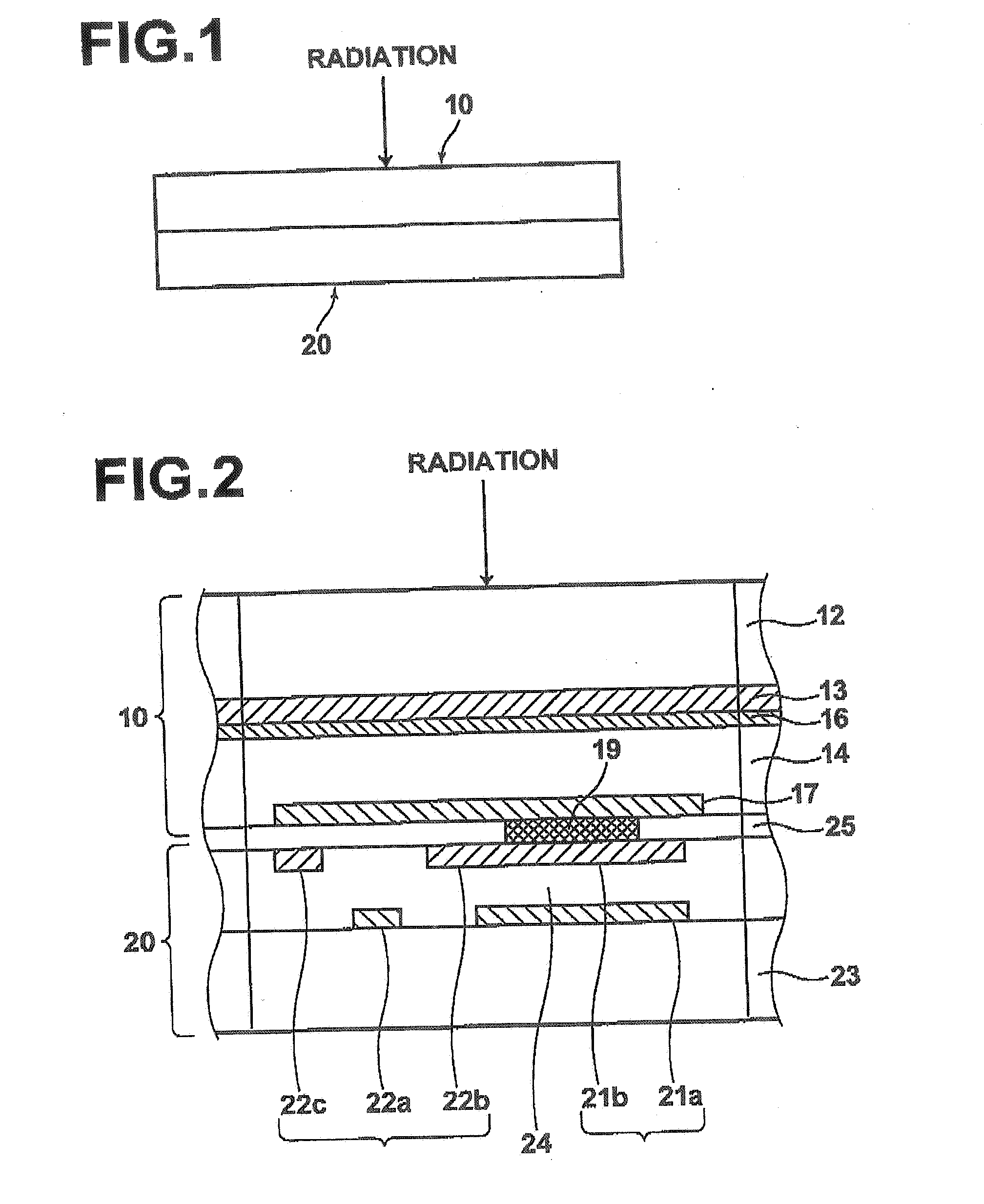
[0015]The radiation detecting system of the present invention, since an organic resin dielectric layer which is not smaller than 0.01 μm and smaller than 1 μm in thickness, not lower than 1012 Ωcm in specific resistance and 6×10⁻⁶ to 1.5×10⁻⁴ / ° C. in thermal expansion coefficient is provided between the recording photoconductive layer and the electric voltage imparting electrode in a radiation detecting system having a recording photoconductive layer which comprises a-Se and generates electric charges in response to receipt of projection of radiation, can give rectifying characteristics to the interface of the voltage imparting electrode and the photoconductive layer and reduce the dark current without deteriorating the sensitivity and at the same time, suppress peeling off on the interfaces of the voltage imparting electrode and the photoconductive layer and of the organic resin dielectric layer and the electric voltage imparting electrode.

Problems solved by technology

Further, there is a problem that, when the carrier selective semi-insulating layer is formed over the recording photoconductive layer of a-Se by deposition, the a-Se layer is crystallized under the heat of the deposition, which leads to generation of image defect, generation of noise, and deterioration of S / N ratio.
Further, when Sb2S3 layer is formed as the carrier selective semi-insulating layer, the large difference in the thermal expansion coefficient between the carrier selective semi-insulating layer and a-Se layer can make cracks in the Sb2S3 layer due to change in the environmental temperature and warpage of the substrate.

Method used


Image

  • Radiation detecting system
  • Radiation detecting system
  • Radiation detecting system

Examples


examples

[0039]Radiation detecting systems were produced by bonding a radiation detecting portion, comprising an electric voltage imparting electrode of Au to which a bias voltage was applied, an organic resin dielectric layer of material and thickness shown in table 1, a recording photoconductive layer of a-Se 1000 μm thick and a carrier collecting electrode of ITO (In2O3:Sn) superposed one on another in this order, to the above described switching element. Further, in embodiment 3 and comparative example 1, there were respectively produced radiation detecting systems which further comprised a carrier selective semi-insulating layer of Sb2S3 between the organic resin dielectric layer and the electric voltage imparting electrode, and a carrier selective semi-insulating layer of Sb2S3 with no organic resin dielectric layer.

[0040]Dark current, deterioration in sensitivity, the thermal expansion coefficient of the organic resin dielectric layer and film stability of the produced radiation detec...


PUM


Abstract

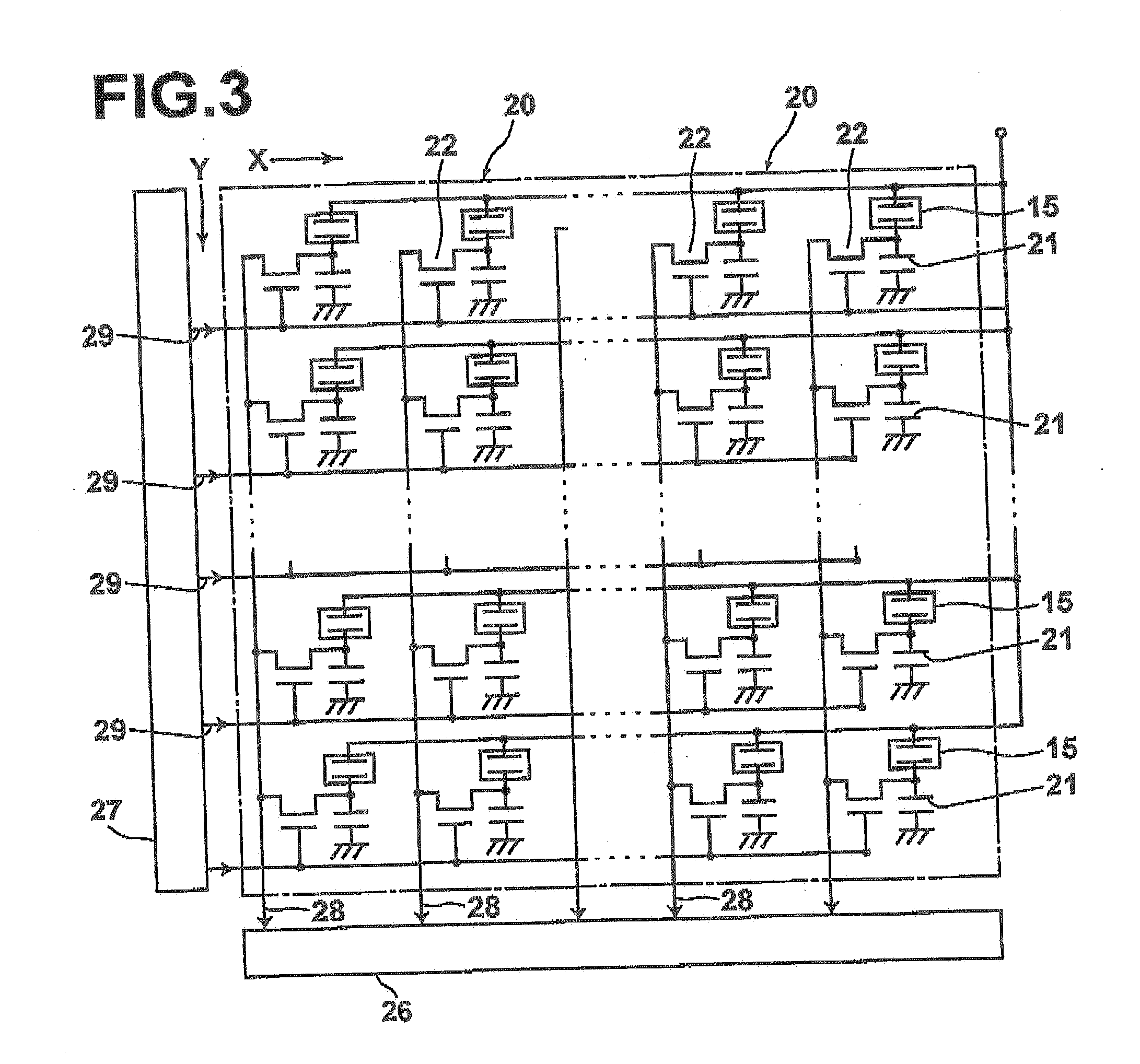
In a radiation detecting system including an electric voltage imparting electrode through which a bias electric voltage is applied, a recording photoconductive layer which comprises a-Se and generates electric charges in response to receipt of projection of radiation, a carrier collecting electrode, a charge storing portion which stores electric charges generated in the recording photoconductive layer and a switching element for reading out charge signal stored in the charge storing portion, superposed one on another in this order, an organic resin dielectric layer which is not smaller than 0.01 μm and smaller than 1 μm in thickness, not lower than 1012 Ωcm in specific resistance and 6×10⁻⁶ to 1.5×10⁻⁴ / ° C. in thermal expansion coefficient is provided between the recording photoconductive layer and the electric voltage imparting electrode.

Description

BACKGROUND OF THE INVENTION[0001]1. Field of the Invention[0002]This invention relates to a radiation detecting system suitable for applying to a radiation image taking system such as an X-ray system, and more particularly to a direct-conversion type radiation detecting system.[0003]2. Description of the Related Art[0004]In the medical radiation image taking, there has been known a radiation detecting system using a radiation sensor (having semiconductor as a main component) which detects radiation and converts it to an electric signal. As the radiation sensor, there has been known those of a direct conversion system where radiation is directly converted to electric charges and the electric charges are stored and an indirect conversion system where radiation is once converted to light by a scintillator or the like, the light is converted to electric charges by a photoconductive layer and the electric charges are stored. From the reading system, the radiation sensor is broadly divide...

Claims


Application Information

Patent Timeline
IPC IPC(8): G01T1/24
CPCG01T1/244
Inventor NARIYUKI, FUMITOIMAI, SHINJI
Owner FUJIFILM CORP
Learn More