
Pulse modulated charge pump circuit

a charge pump and pulse technology, applied in pulse techniques, generating/distributing signals, instruments, etc., can solve the problems of reducing the width of the gate is reduced, and the bandwidth of the switch is lower, so as to achieve the effect of increasing the voltage of the transmission ga

Inactive Publication Date: 2010-06-17
INTEGRATED DEVICE TECH INC
View PDF11 Cites 13 Cited by
  • Summary
  • Abstract
  • Description
  • Claims
  • Application Information

AI Technical Summary

Benefits of technology

[0009]In accordance with aspects of the present invention, there is also provided a circuit for increasing a gate voltage of a transmission gate in a high-speed switch to a voltage higher than a level of a supply voltage, comprising an oscillator generating a clock signal; a charge pump circuit operatively coupled to the oscillator, the charge pump circuit receiving the supply voltage and the clock signal as inputs and outputting the gate voltage; a comparator circuit coupled to the oscillator circuit and the charge pump circuit; and a pulse signal generator circuit operatively coupled to the oscillator, the pulse signal generator circuit generating a pulse signal to enable the oscillator and modulate the charge pump circuit.
[0010]In accordance with aspects of the present invention there is further provided a method of increasing a voltage of a transmission gate in a high-speed switch, comprising generating a pulse signal at a predetermined or adaptive frequency and pulse width; generating a clock signal at predetermined intervals in response to the generated pulse signal; and increasing the voltage of the transmission gate in response to the generated clock voltage.

Problems solved by technology

However, increased gate width also means increased parasitic capacitance of the switch, which may result in the switch having lower bandwidth.
However, this often results in a gate having a reduced gate width, and a higher on resistance.
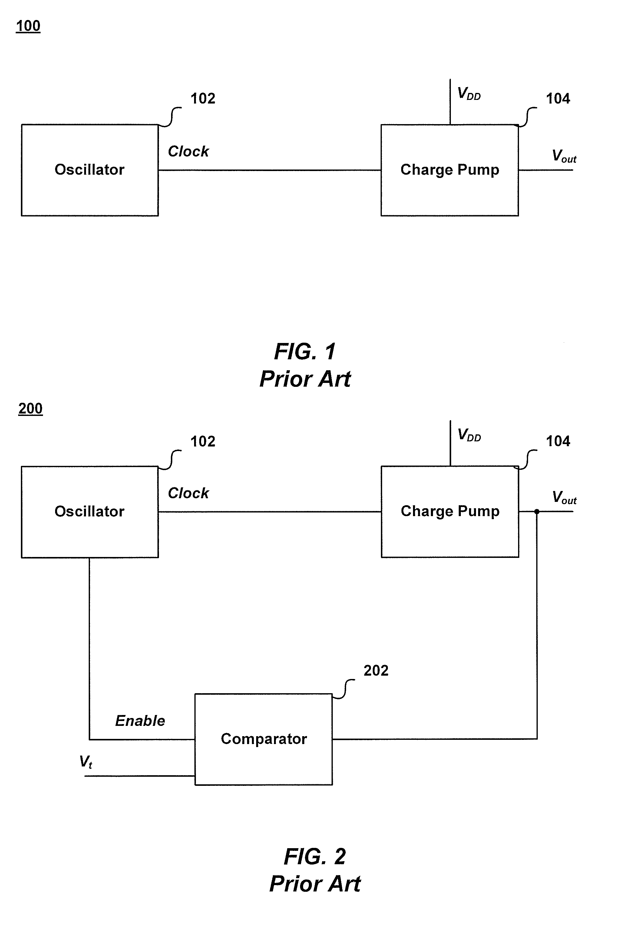
However, in using the configuration shown in FIG. 1, it is difficult to regulate output voltage Vout.
Therefore, the power consumption of circuit 100, and therefore circuit 100, is typically very inefficient.
However, in voltage pumping circuit 200, comparator 202 is constantly operating, comparing output voltage Vout with target voltage Vt, and thus is continually consuming power.

Method used


Image

  • Pulse modulated charge pump circuit
  • Pulse modulated charge pump circuit
  • Pulse modulated charge pump circuit

Examples


Embodiment Construction

[0019]In the following description specific details are set forth describing certain embodiments of the invention. It will be apparent, however, to one skilled in the art that the present invention may be practiced without some or all of these specific details. The specific embodiments presented are meant to be illustrative of the present invention, but not limiting. One skilled in the art may realize other material that, although not specifically described herein, is within the scope and spirit of this disclosure.

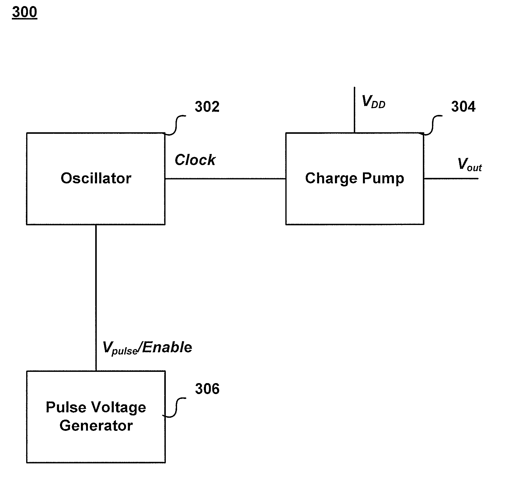
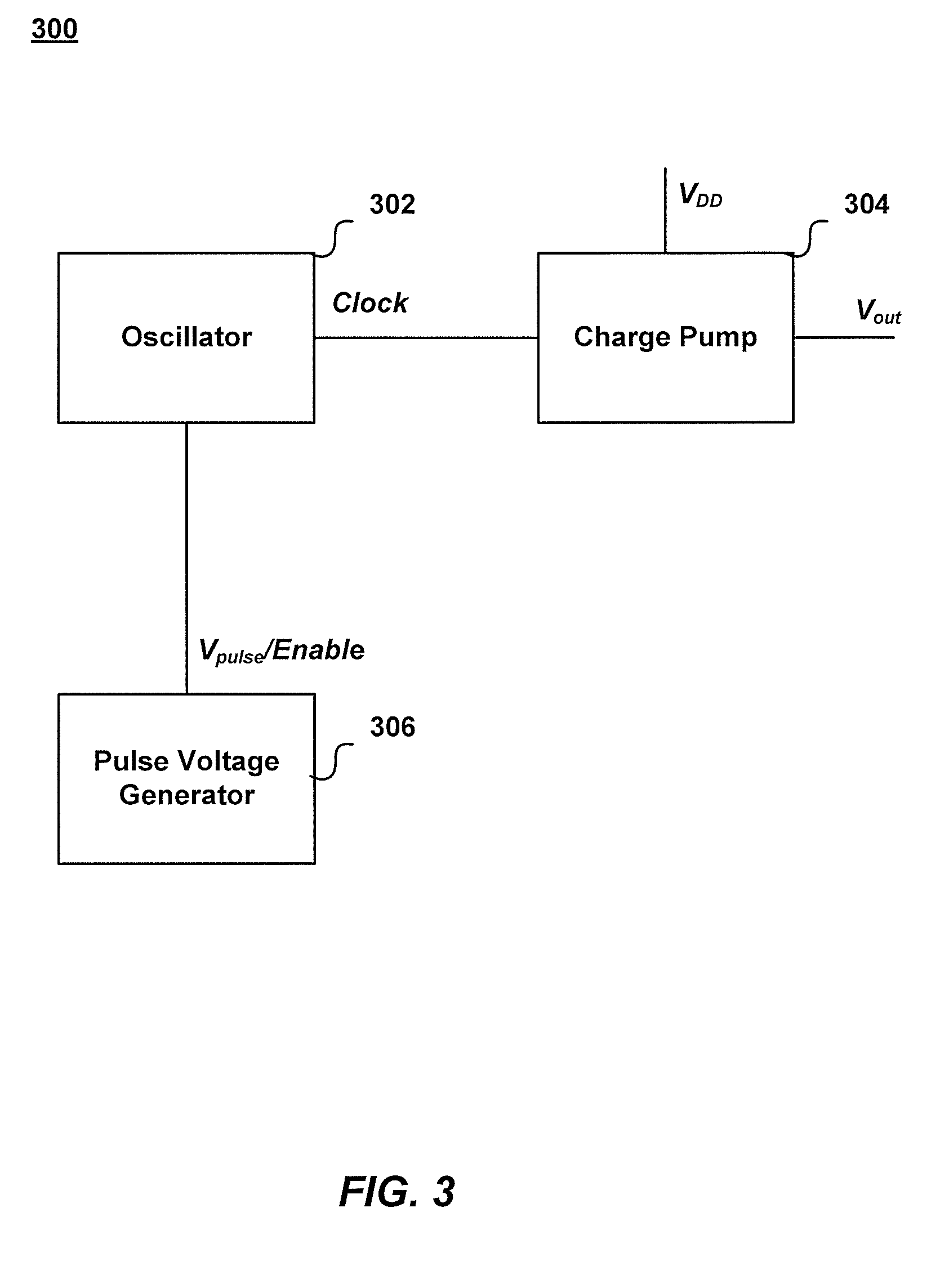
[0020]FIG. 3 is a diagram illustrating a voltage pumping circuit 300 according to an embodiment consistent with the present invention. As shown in FIG. 3, voltage pumping circuit 300 includes an oscillator 302 coupled to a charge pump circuit 304. Charge pump circuit 304 receives a clock signal from the oscillator and a supply voltage VDD, and outputs an output voltage Vout having a higher level than VDD. Voltage pumping circuit 300 also includes a pulse voltage generator ...


PUM


Abstract

A circuit for increasing a gate voltage of a transmission gate in a high-speed switch to a level higher than a level of a supply voltage is provided. The circuit includes an oscillator generating a clock signal and a charge pump circuit operatively coupled to the oscillator. The charge pump circuit receives the supply voltage and the clock signal as inputs, and outputs the gate voltage. The circuit also includes a comparator circuit coupled to the oscillator circuit and the charge pump circuit and a pulse signal generator circuit operatively coupled to the oscillator, the pulse signal generator circuit generating a pulse signal which enables the oscillator.

Description

TECHNICAL FIELD[0001]The present invention is related to increasing the voltage of a transmission gate in a high-speed switch, and, in particular, to a pulse modulated charge pump.DISCUSSION OF RELATED ART[0002]In typical high-speed switch design, a transmission gate is often used. A transmission gate is typically a CMOS-type switch which uses one PMOS and one NMOS FET connected in parallel, wherein the gate voltage controls the operation of the switch. The on resistance of the switch is proportional to the width of the gate and the drive voltage of the gate. However, increased gate width also means increased parasitic capacitance of the switch, which may result in the switch having lower bandwidth. Accordingly, to decrease the parasitic capacitance, and, in turn increase the bandwidth of the transmission gate an NMOS FET is most often used in the transmission gate in high speed applications. However, this often results in a gate having a reduced gate width, and a higher on resistan...

Claims


Application Information

Patent Timeline
Patent Type & Authority Applications(United States)
IPC IPC(8): G05F1/10G06F1/04
CPCH02M3/073
Inventor WENG, SIYOUISIK, TACETTIN
Owner INTEGRATED DEVICE TECH INC
Learn More