
Test fail analysis on VLSI chips

a technology of test failure and chip, applied in semiconductor/solid-state device testing/measurement, image enhancement, instruments, etc., can solve problems such as difficult identification and mapping of test failures, process variations in the chip fabric, and test failures that can happen

Inactive Publication Date: 2010-06-03
IBM CORP
View PDF14 Cites 6 Cited by
  • Summary
  • Abstract
  • Description
  • Claims
  • Application Information

AI Technical Summary

Problems solved by technology

Process related chip test issues are difficult to identify and map to test fails at the chip tester by the test engineer who normally is not a process engineer.
When such a chip is tested in a fabric test environment, some test fails can happen.
However, there are process variations in the chip fabric that are not necessarily fed back or reflected in the test model for the device or design under test.
This leads to slightly changing test fail signatures over time and over the wide process range or tolerances for such a device under test.

Method used


Image

  • Test fail analysis on VLSI chips
  • Test fail analysis on VLSI chips
  • Test fail analysis on VLSI chips

Examples


Embodiment Construction

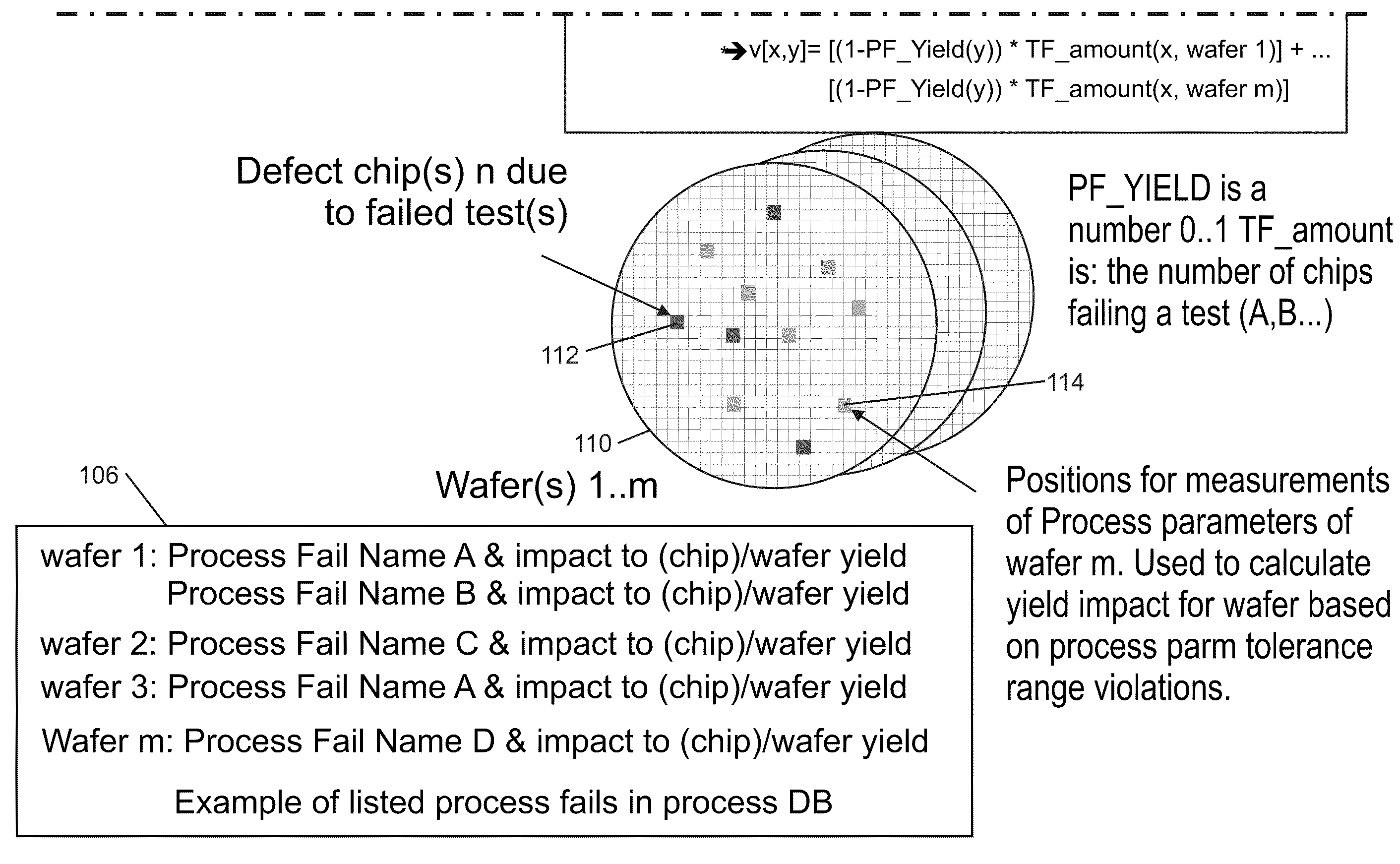
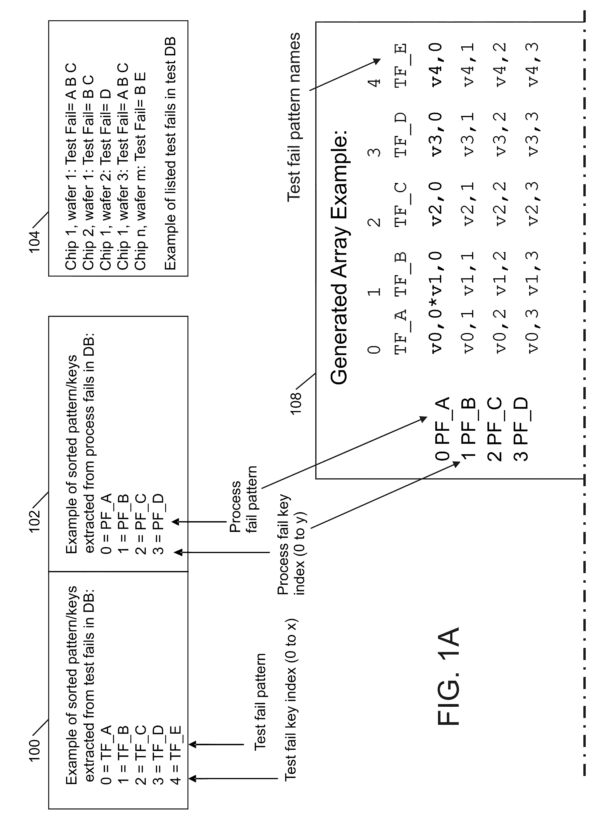
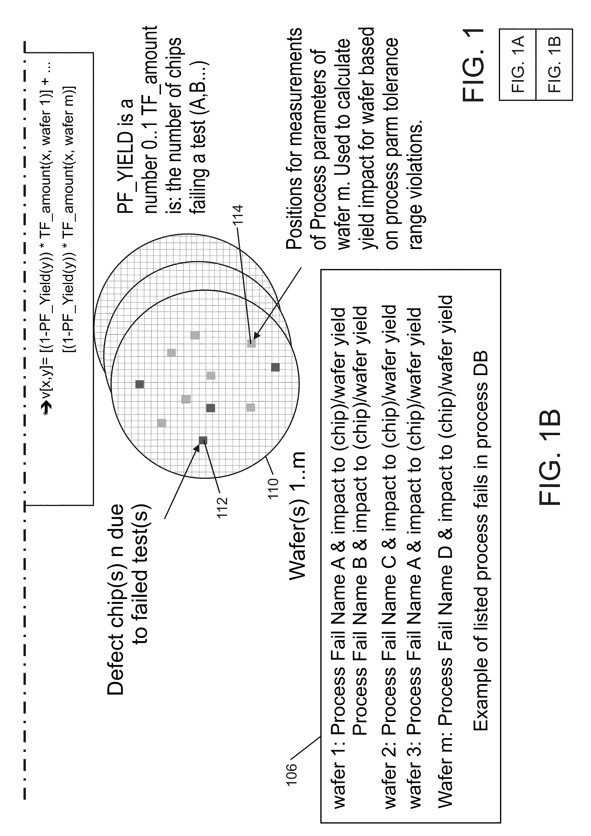
[0020]Referring to FIG. 1, there illustrated is an exemplary embodiment of the mechanics of process fail to test fail analysis and determination. As used herein, a test fail generally refers to an issue with the design of the chip or integrated circuit (IC), while a process fail generally refers to an issue with a physical reference on or associated with the chip, for example, the length of a transistor channel. In a block 100 in FIG. 1 there is a listing of an example of sorted pattern / keys extracted from a list of test fails in a database. The chip testing device typically creates a database for each chip that undergoes testing and the database gives test behavioral characteristics of the chip during the testing process (i.e., whether there were any test fails and / or process fails). The listing assigns a test fail key index number of from 0 to x (where x+1 is a maximum number of tests performed on a chip) to a listing of different test fail pattern names (e.g., TF_A. TF_B, etc.). ...


PUM


Abstract

Compact graphical representations of common test fail signatures and process related test fails are provided through methods of selecting, calculating and / or presenting information. The input may be a list of failing tests on a sample of devices under test from chip and / or wafer process fails. The failing tests are identified and then other tests that fail at the same time may be identified. Several graphical outputs are provided, including all possible combinations between test fails and between test fails and process fails. The dependencies are printed as sorted two dimensional bitmaps that are compact representations of the results using color codes. Subtraction of two independent bitmaps is provided, which eliminates common properties and emphasizes differences between multiple bitmaps which allows for quick identification of differences of process fails potentially different between the two different bitmaps indicating potential root causes for the selected one of the test fails.

Description

BACKGROUND[0001]The present invention relates to semiconductor manufacturing technology, and, more specifically, to the analysis and determination of potential process driven test fails during very large scale integrated circuit (VLSI) chip testing and to finding common test fail signatures when running different test patterns indicating potential redundant test patterns.[0002]Process related chip test issues are difficult to identify and map to test fails at the chip tester by the test engineer who normally is not a process engineer. Identified dependencies between test fails and process fails allow one to determine whether chip test fails are somehow related to process fails coming from production. Especially in the design phase of VLSI chip components, it is more often the case that circuit designs are used in test chips or intermittent design levels of product chips without having final product quality. When such a chip is tested in a fabric test environment, some test fails can...

Claims


Application Information

Patent Timeline
Patent Type & Authority Applications(United States)
IPC IPC(8): G06K9/00
CPCG06T2207/30148G06T7/001H01L22/00G01R31/26
Inventor ECKERT, MARTINGOECKE, GEORGJUNGINGER, MARTAKEMPTER, KLAUSULBRICHT, MARKUS
Owner IBM CORP
Learn More