Method for adjusting capacitance of capacitors without affecting die area

a technology of capacitors and capacitance, which is applied in the field of semiconductor wafer fabrication of capacitors, can solve the problems of undesired increase in manufacturing cost of capacitors, undesirable change in the die area consumed by capacitors, and capacitor layou

Active Publication Date: 2010-05-27
AVAGO TECH INT SALES PTE LTD
View PDF3 Cites 23 Cited by
  • Summary
  • Abstract
  • Description
  • Claims
  • Application Information

AI Technical Summary

Benefits of technology

[0007]A method for adjusting capacitance of capacitors without affecting die area substantially as shown in and / or described in connection with at least one of the figures, as set forth more completely in the claims.

Problems solved by technology

However, for a variety of reasons, the process parameters utilized to fabricate a capacitor in one foundry may not match the process parameters utilized to fabricate the capacitor in another foundry, thereby causing the capacitor to have a different capacitance value in each foundry.
However, manually redesigning the layout of the capacitor can undesirably increase manufacturing cost and requires the data files, such as such as Graphic Data System (GDS) data files including the layout of the capacitor, to be regenerated for “tape-out” to the production foundry.
Moreover, according to conventional approaches, redesigning the capacitor layout usually causes an undesirable change in the die area consumed by the capacitor.

Method used


Image

  • Method for adjusting capacitance of capacitors without affecting die area
  • Method for adjusting capacitance of capacitors without affecting die area
  • Method for adjusting capacitance of capacitors without affecting die area

Examples


Embodiment Construction

[0014]The present invention is directed to a method for adjusting capacitance of capacitors without affecting die area. The following description contains specific information pertaining to the implementation of the present invention. One skilled in the art will recognize that the present invention may be implemented in a manner different from that specifically discussed in the present application. Moreover, some of the specific details of the invention are not discussed in order not to obscure the invention.

[0015]The drawings in the present application and their accompanying detailed description are directed to merely exemplary embodiments of the invention. To maintain brevity, other embodiments of the present invention are not specifically described in the present application and are not specifically illustrated by the present drawings.

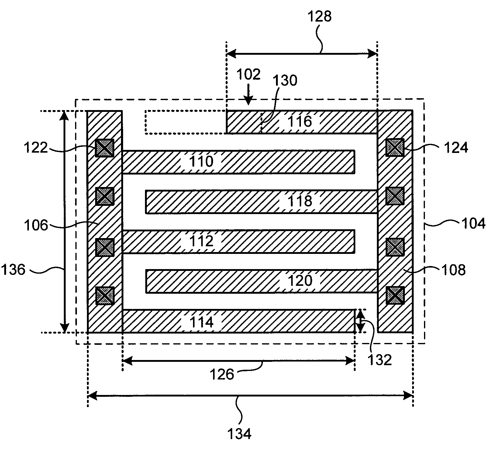
[0016]FIG. 1 shows a top view of capacitor 102 in standard cell 104 in accordance with one embodiment of the present invention. Capacitor 102, whic...


PUM

PropertyMeasurementUnit
capacitanceaaaaaaaaaa
lengthaaaaaaaaaa
conductiveaaaaaaaaaa

Abstract

According to one exemplary embodiment, a method for adjusting geometry of a capacitor includes fabricating a first composite capacitor residing in a first standard cell with a first set of process parameters. The method further includes using a second standard cell having substantially same dimensions as the first standard cell. The method further includes using a capacitance value from the first composite capacitor to adjust a geometry of a second composite capacitor residing in the second standard cell, wherein the second composite capacitor is fabricated with a second set of process parameters. The geometry of the second composite capacitor can be adjusted to cause the second composite capacitor to have a capacitance value substantially equal to the capacitance value from the first composite capacitor.

Description

BACKGROUND OF THE INVENTION[0001]1. Field of the Invention[0002]The present invention is generally in the field of semiconductors. More specifically, the present invention is in the field of fabrication of capacitors in semiconductor wafers.[0003]2. Background Art[0004]Various types of capacitors, such as composite capacitors comprising several interconnected capacitors, are used in circuits in semiconductor devices, such as mixers and amplifiers, and are required to provide high capacitance density without consuming a large area on a semiconductor die (also referred to simply as a “die”). A composite capacitor can include multiple stacked layers, where each layer of the capacitor can reside in a different metal layer of a die and be electrically connected to other capacitor layers by vias. During a typical design cycle, a circuit layout design including a capacitor, such as a composite capacitor, can be verified by fabricating the circuit including the capacitor in a small-scale en...

Claims


Application Information

Patent Timeline
Patent Type & Authority Applications(United States)
IPC IPC(8): H01G7/00
CPCH01G4/33Y10T29/435H01L27/0207H01L22/20H01L22/14H01L27/118H01L28/86
Inventor HUANG, PETERCHEN, MING-CHUN
Owner AVAGO TECH INT SALES PTE LTD
Why Eureka
Try Eureka