
Photonics device

a technology of photonics and filters, applied in the field of photonics devices, can solve the problems of difficult to maintain the wavelength spacing between channels of a ring resonator or awg at a constant level, and it is difficult to fabricate the ring resonator or the awg stably through a photolithography process using an arf excimer laser having a wavelength of 193 nm, so as to increase the effective refractive index

Inactive Publication Date: 2010-05-06
ELECTRONICS & TELECOMM RES INST
View PDF8 Cites 0 Cited by
  • Summary
  • Abstract
  • Description
  • Claims
  • Application Information

AI Technical Summary

Benefits of technology

[0007]The present invention also provides a photonics device having improved inter-channel wavelength spacing characteristics.
[0009]The present invention also provides a photonics device that can have stable characteristics even when fabricated using an ArF excimer laser.

Problems solved by technology

However, since a ring resonator or an AWG is highly sensitive to statistic errors caused by inevitable process condition variations, it is difficult to maintain wavelength spacing between channels of a ring resonator or an AWG at a constant level.
Moreover, since the ring resonator or the AWG has a minimum line width of about 100 nm, it is difficult to fabricate the ring resonator or the AWG stably through a photolithography process using an ArF excimer laser having a wavelength of 193 nm.

Method used


Image

  • Photonics device
  • Photonics device
  • Photonics device

Examples


Embodiment Construction

[0024]Preferred embodiments of the present invention will be described below in more detail with reference to the accompanying drawings. The present invention may, however, be embodied in different forms and should not be construed as limited to the embodiments set forth herein. Rather, these embodiments are provided so that this disclosure will be thorough and complete, and will fully convey the scope of the present invention to those skilled in the art.

[0025]In the specification, the dimensions of layers and regions are exaggerated for clarity of illustration. It will also be understood that when a layer (or film) is referred to as being ‘on’ another layer or substrate, it can be directly on the other layer or substrate, or intervening layers may also be present. Also, though terms like a first, a second, and a third are used to describe various regions and layers in various embodiments of the present invention, the regions and the layers are not limited to these terms. These term...


PUM


Abstract

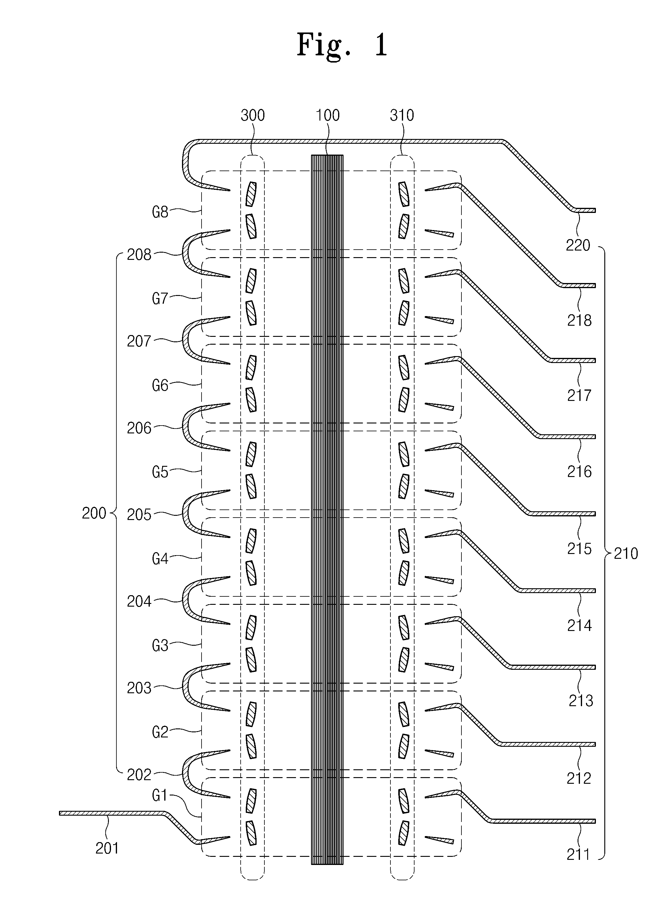
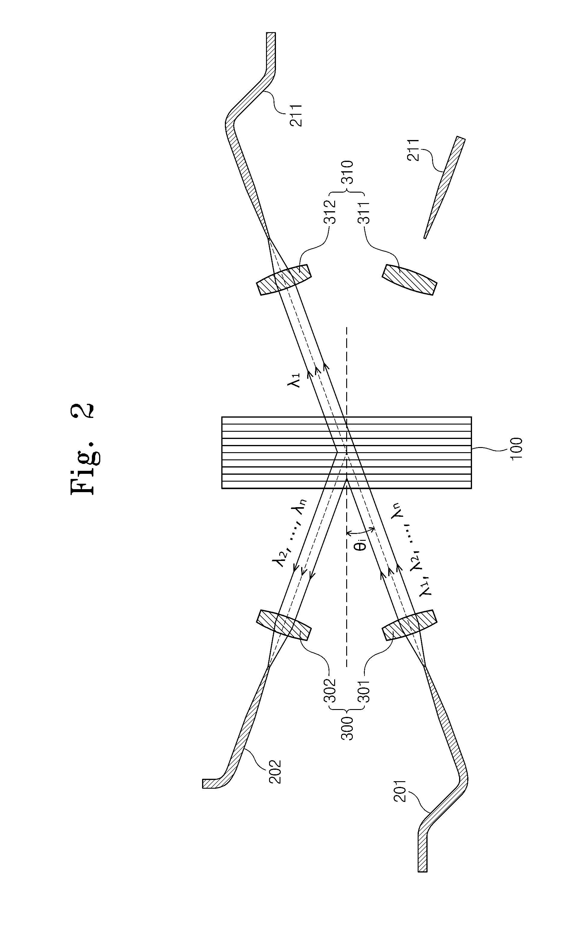
Provided is a photonics device. The photonics device includes a distribution Bragg reflector (DBR), first and second waveguides disposed at both sides of the DBR, first lenses disposed between the DBR and the first waveguides, and second lenses disposed between the DBR and the second waveguides.

Description

CROSS-REFERENCE TO RELATED APPLICATIONS[0001]This U.S. non-provisional patent application claims priority under 35 U.S.C. § 119 of Korean Patent Application No. 10-2008-010830, filed on Nov. 3, 2008, the entire contents of which are hereby incorporated by reference.BACKGROUND OF THE INVENTION[0002]The present invention disclosed herein relates to a photonics device, and more particularly, to a multi-channel distribution Bragg reflector (DBR) filter.[0003]In twenty-first century, optical communication technology has been highly developed, and much research is currently underway to apply optical communication technology to communication between computer boards, communication between chips of a board, or communication inside a complementary metal oxide semiconductor (CMOS) chip. In the case where optical signal communication technology is applied to a silicon very-large-scale-integration circuit (VLSI) chip, demerits of electric signal communication technology such as low-speed, high-r...

Claims


Application Information

Patent Timeline
Patent Type & Authority Applications(United States)
IPC IPC(8): G02B5/18
CPCG02B6/264G02B6/305G02B6/32G02B6/12
Inventor PARK, SAHNGGIKIM, KAP-JOONGKIM, IN-GYOOKIM, GYUNGOCK
Owner ELECTRONICS & TELECOMM RES INST
Learn More