
Etch reactor suitable for etching high aspect ratio features

a technology of etch reactor and high aspect ratio, which is applied in the direction of electrical equipment, contact engagements, electric discharge tubes, etc., to achieve the effect of high aspect ratio and high features

Inactive Publication Date: 2010-04-22
APPLIED MATERIALS INC
View PDF12 Cites 65 Cited by
  • Summary
  • Abstract
  • Description
  • Claims
  • Application Information

AI Technical Summary

Benefits of technology

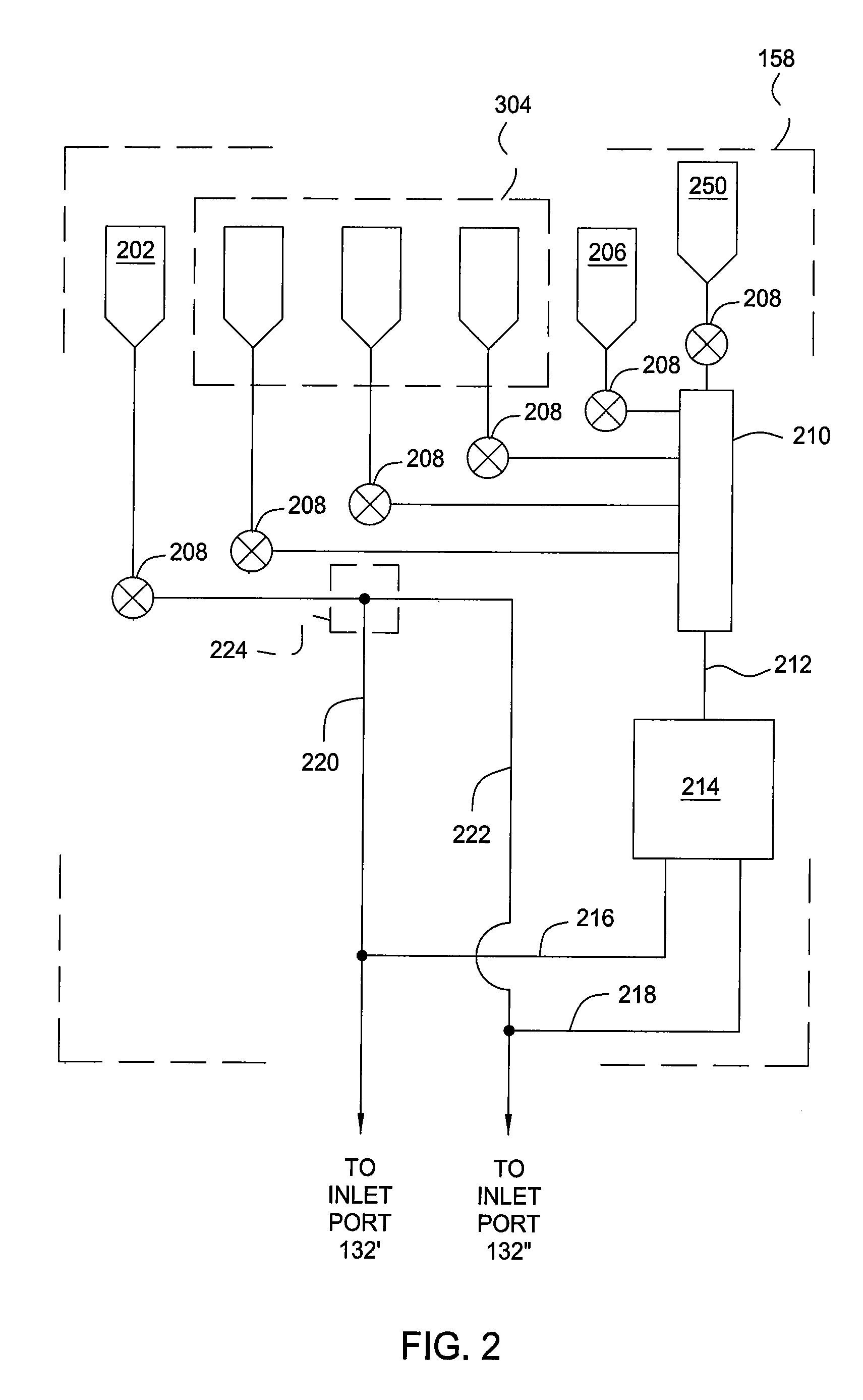
[0008]Embodiments of the invention provide a method and apparatus that enables plasma etching of high aspect ratio features. In one embodiment, an apparatus for plasma etching is provided. The processing chamber includes a chamber body having an interior volume, a showerhead assembly coupled to a ceiling of the chamber body, the showerhead assembly configured to deliver a gas mixture from at least two isolated locations into the chamber body, a substrate support assembly disposed in the chamber body, at least two RF power sources coupled to the substrate support assembly, a bias power source coupled to the substrate support assembly, and a controller interfaced with instructions stored in a memory, the instructions, when executed by the controller, causes a method to be preformed in the processing chamber, the method includes providing the gas mixture through the showerhead assembly into the chamber body, applying RF power to maintain a

Problems solved by technology

The demand for faster, more powerful integrated circuits (IC) devices has introduced new challenges for IC fabrication technology, including the need to etch high aspect ratio of features such as trenches or vias on a substrate such as a semiconductor wafer.

Method used


Image

  • Etch reactor suitable for etching high aspect ratio features
  • Etch reactor suitable for etching high aspect ratio features
  • Etch reactor suitable for etching high aspect ratio features

Examples


Embodiment Construction

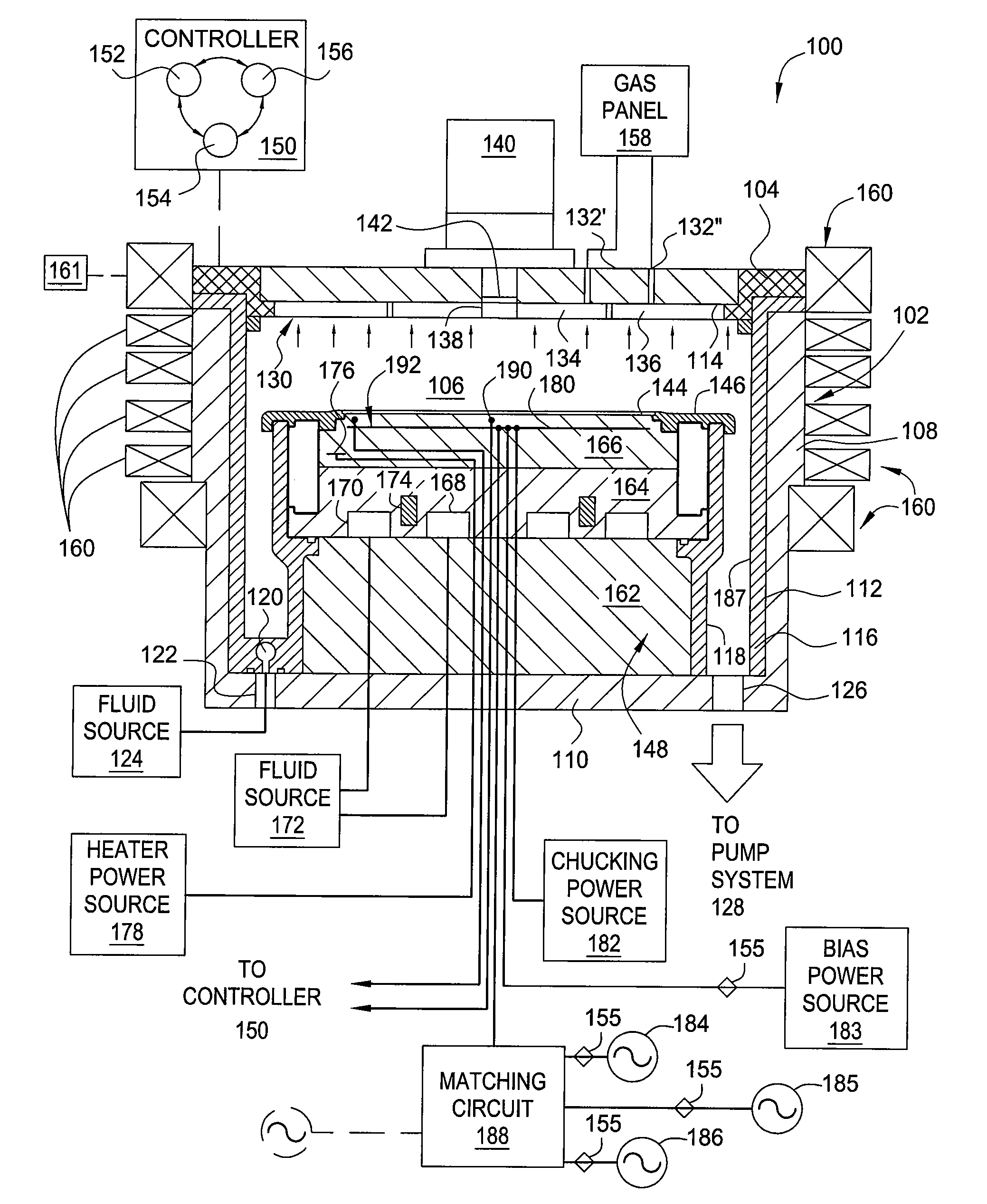
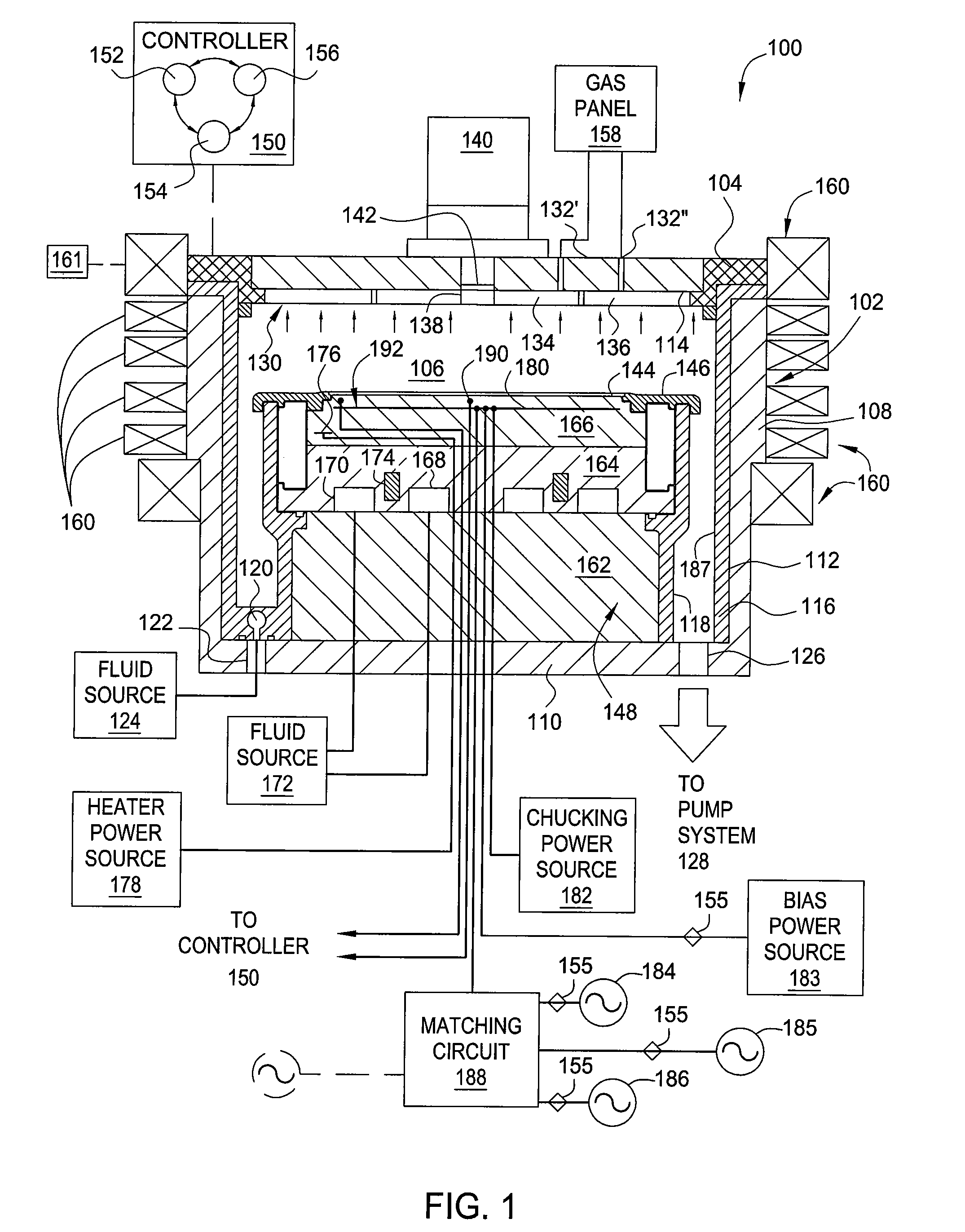
[0015]FIG. 1 is a sectional view of one embodiment of an etch reactor 100 suitable for etching high aspect ratio features in a substrate 144. Although the etch reactor 100 is shown including a plurality of features that enable superior etching performance, it is contemplated that other processing chambers may be adapted to benefit from one or more of the inventive features disclosed herein.

[0016]The etch reactor 100 includes a chamber body 102 and a lid 104 which enclose an interior volume 106. The chamber body 102 is typically fabricated from aluminum, stainless steel or other suitable material. The chamber body 102 generally includes sidewalls 108 and a bottom 110. A substrate access port (not shown) is generally defined in a sidewall 108 and a selectively sealed by a slit valve to facilitate entry and egress of the substrate 144 from the etch reactor 100. An exhaust port 126 is defined in the chamber body 102 and couples the interior volume 106 to a pump system 128. The pump syst...


PUM

PropertyMeasurementUnit
Fractionaaaaaaaaaa
Fractionaaaaaaaaaa
Frequencyaaaaaaaaaa

Abstract

Embodiments of the invention provide a method and apparatus that enables plasma etching of high aspect ratio features. In one embodiment, a method for etching is provided that includes providing a substrate having a patterned mask disposed on a silicon layer in an etch reactor, providing a gas mixture of the reactor, maintaining a plasma formed from the gas mixture, wherein bias power and RF power provided the reactor are pulsed, and etching the silicon layer in the presence of the plasma.

Description

CROSS-REFERENCE TO RELATED APPLICATIONS[0001]This application claims benefit of U.S. Provisional Application Ser. No. 61 / 099,079 filed Sep. 22, 2008 (Attorney Docket No. APPM / 12969L), which is incorporated by reference in its entirety.BACKGROUND[0002]1. Field[0003]Embodiments of the invention generally relate to a vacuum processing chamber for etching high aspect ratio features in semiconductor substrates and the like, and the components utilized therein.[0004]2. Description of the Related Art[0005]The demand for faster, more powerful integrated circuits (IC) devices has introduced new challenges for IC fabrication technology, including the need to etch high aspect ratio of features such as trenches or vias on a substrate such as a semiconductor wafer. For example, deep trench storage structures used in some dynamic random access memory applications require deep high aspect ratio trenches etched into a semiconductor substrate. Deep silicone trench etching is typically carried out in...

Claims


Application Information

Patent Timeline
IPC IPC(8): H01L21/3065C23F1/08
CPCH01J37/32009H01J2237/334H01J37/32045H01H1/34H01L21/3065
Inventor OSWALD, MANFREDDINEV, JIVKORUPF, JANMEYE, MARKUSMALETTA, FRANCESCOLEUCKE, UWETILGER, RONABOOAMERI, FARIDMATYUSHKIN, ALEXANDERKOOSAU, DENISZHOU, XIAOPINGLEHMANN, THORSTENSCANLAN, DECLAN
Owner APPLIED MATERIALS INC
Learn More