Infrared-reflecting films and method for making the same
a technology of infrared reflection and film, applied in the field of infrared reflection films, can solve the problems of not providing all the known films and methods, and achieve the effects of reducing the cost of production, reducing the degradation of materials, and being suitable for industrial-scale manufacturing
- Summary
- Abstract
- Description
- Claims
- Application Information
AI Technical Summary
Benefits of technology
Problems solved by technology
Method used
Image
Examples
example 1
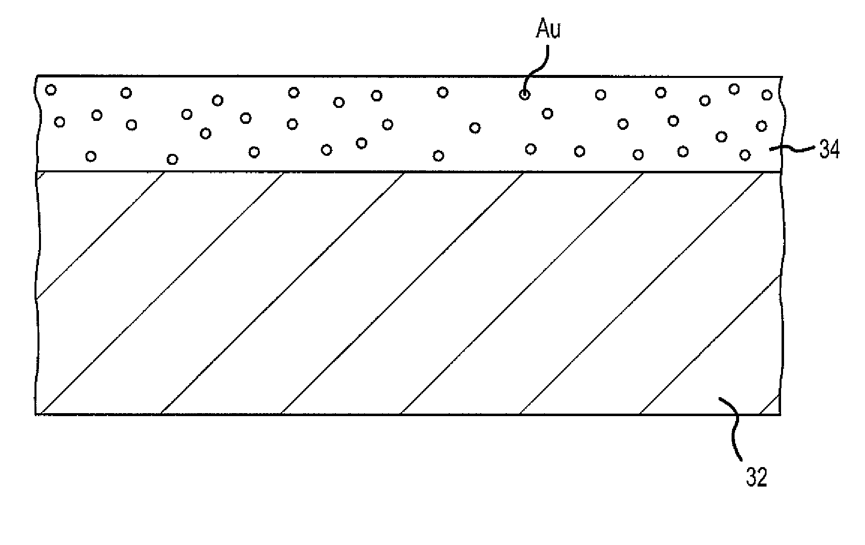
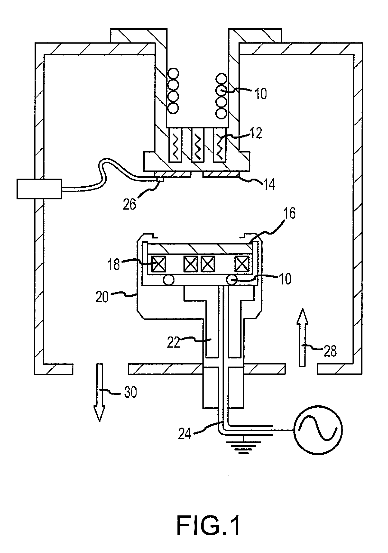
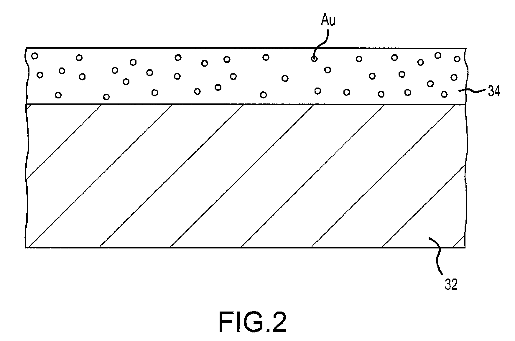
[0033]TiO2 film with gold (Au) was synthesized by magnetron sputtering onto a silicon substrate and glass cover slip. The substrate was ultrasonically cleaned in acetone for 15 minutes followed by cleaning in methanol for 15 minutes. The substrate was then placed in a vacuum chamber, with a base pressure of less than 5.0×10⁻⁸ Torr. The substrate was sputter-cleaned at a voltage of −150 Volts (V) in an argon atmosphere of 50 mTorr for 5 minutes. Then the deposition was carried out at 175 Watts (W) of power on a 2-inch diameter titanium target with inserted Au wires, pulsing at 250 kiloHertz (kHz). The substrate bias during deposition was −150 V, pulsing at 150 kHz. The sputtering atmosphere was 75% argon and 25% oxygen, with a total pressure of 5 mTorr. Final film thickness was around 300 nm (0.3 micron) to 500 nm (0.5 micron). Because of problems associated with oxygen flow control in some experiments, the TiO2 films were often substoichiometric. This problem was solved by annealing...
example 2
[0036]TiO2 film with niobium (Nb) was synthesized by magnetron sputtering onto a silicon substrate and glass cover slip. The substrate was ultrasonically cleaned in acetone for 15 minutes followed by cleaning in methanol for 15 minutes. The substrate was then placed in a vacuum chamber, with a base pressure of less than 5.0×10⁻⁸ Torr. The substrate was sputter-cleaned at a voltage of −150 Volts (V) in an argon atmosphere of 50 mTorr for 5 minutes. Then the deposition was carried out at 175 Watts (W) of power on a 2-inch diameter titanium target with inserted Nb wires, pulsing at 250 kiloHertz (kHz). The substrate bias during deposition was −150V, pulsing at 150 kHz. The sputtering atmosphere was 75% argon and 25% oxygen, with a total pressure of 5 mTorr. Final film thickness was around 300 nm (0.3 micron) to 500 nm (0.5 micron). Because of problems associated with oxygen flow control in some experiments, the TiO2 films were often substoichiometric. This problem was solved by anneali...
PUM
| Property | Measurement | Unit |
|---|---|---|
| Thickness | aaaaa | aaaaa |
| Thickness | aaaaa | aaaaa |
| Nanoscale particle size | aaaaa | aaaaa |
Abstract
Description
Claims
Application Information
 - R&D
- Intellectual Property
- Life Sciences
- Materials
- Tech Scout
- Unparalleled Data Quality
- Higher Quality Content
- 60% Fewer Hallucinations
Browse by: Latest US Patents, China's latest patents, Technical Efficacy Thesaurus, Application Domain, Technology Topic, Popular Technical Reports.
© 2025 PatSnap. All rights reserved.Legal|Privacy policy|Modern Slavery Act Transparency Statement|Sitemap|About US| Contact US: help@patsnap.com


