Printed circuit board and method of manufacturing the same

a technology of printed circuit boards and manufacturing methods, applied in the field of printed circuit boards, can solve the problems of increasing manufacturing time and production costs, increasing overall manufacturing costs, and solving problems, and achieve the effects of simplifying the process, reducing manufacturing costs, and shortening manufacturing tim

Inactive Publication Date: 2010-03-04
SAMSUNG ELECTRO MECHANICS CO LTD
View PDF4 Cites 7 Cited by
  • Summary
  • Abstract
  • Description
  • Claims
  • Application Information

AI Technical Summary

Benefits of technology

[0008]The present invention provides a printed circuit board and a method of manufacturing the printed circuit board in which the manufacturing time can be shortened and the manufacturing costs can be reduced by simplifying the process.

Problems solved by technology

However, in case these conventional technologies are followed, there may be several problems to be solved.
Firstly, while forming a circuit pattern and a pad, the whole process may become complicated due to the performing of the exposing and developing processes, thereby increasing manufacturing time and production costs.
Secondly, due to an additional cost needed to make a mask for each process, the overall manufacturing costs may be increased.

Method used


Image

  • Printed circuit board and method of manufacturing the same
  • Printed circuit board and method of manufacturing the same
  • Printed circuit board and method of manufacturing the same

Examples


Embodiment Construction

[0024]In accordance with certain embodiments of the present invention, a printed circuit board and a method of manufacturing the printed circuit board will be described below in more detail with reference to the accompanying drawings. Those components that are the same or are in correspondence are rendered the same reference numeral regardless of the figure number, and redundant explanations are omitted.

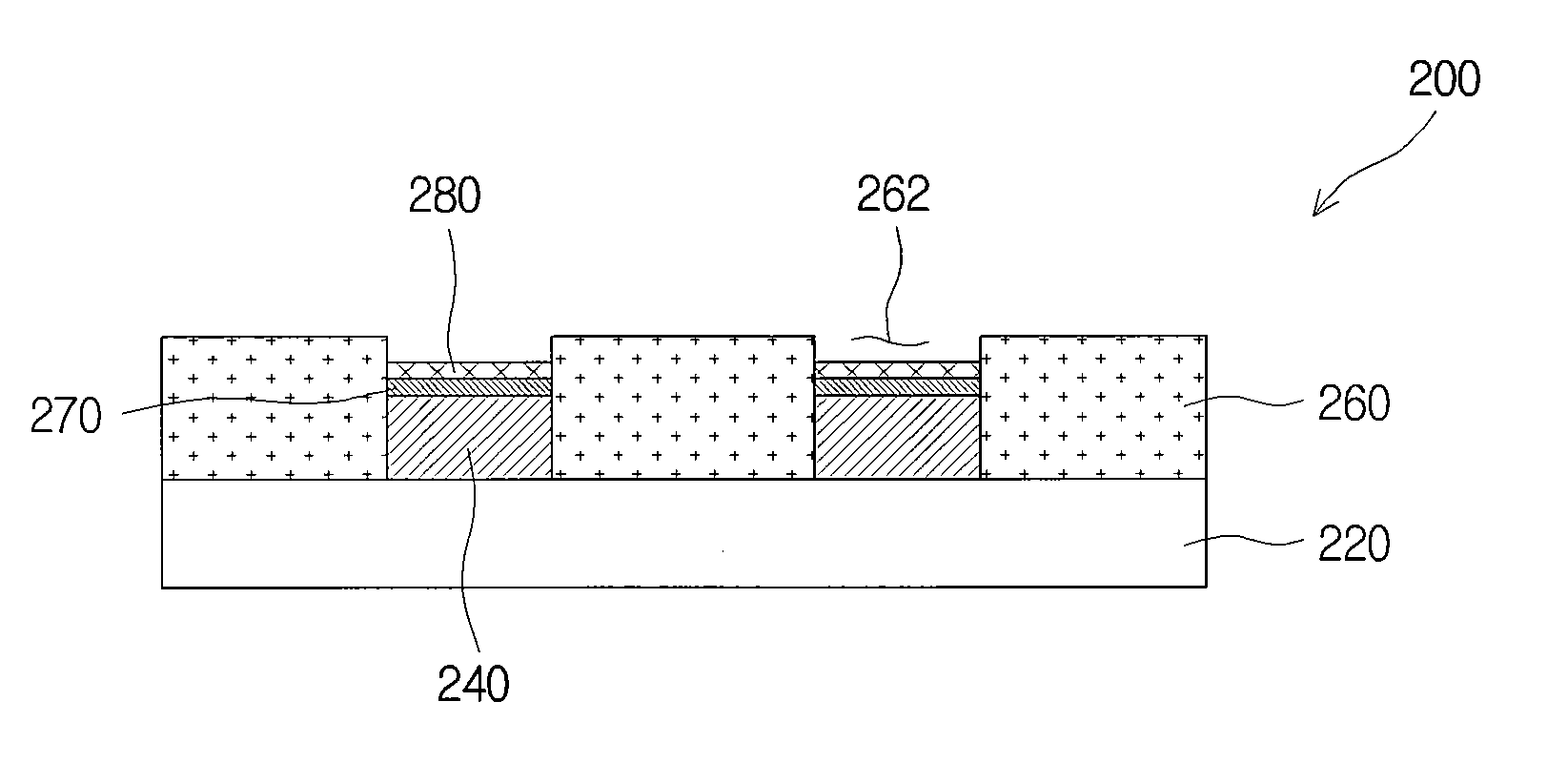
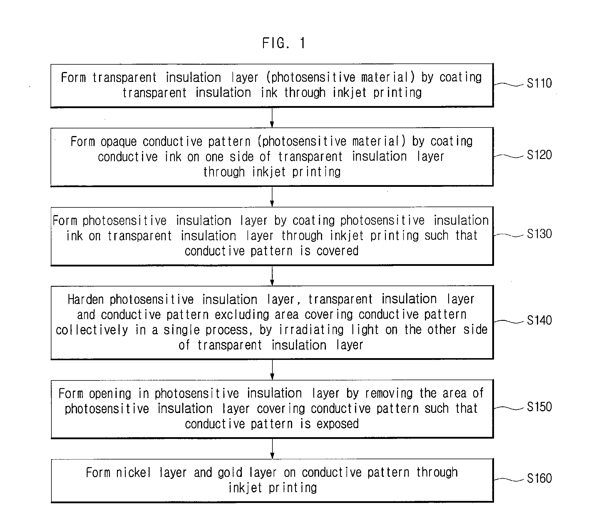
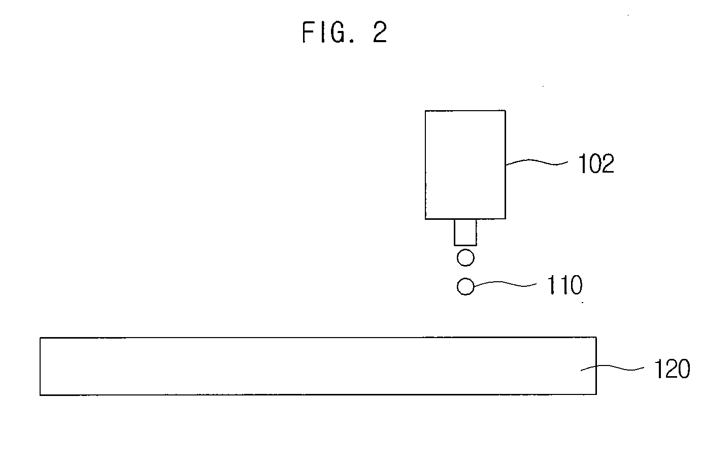
[0025]FIG. 1 is a flow chart illustrating a method of manufacturing a printed circuit board 100 in accordance with an embodiment of the present invention. FIGS. 2 to 7 are cross sectional views illustrating a method of manufacturing the printed circuit board 100 in accordance with an embodiment of the present invention. FIGS. 8 to 13 are plan views illustrating a method of manufacturing the printed circuit board 100 in accordance with an embodiment of the present invention.

[0026]Illustrated in FIGS. 2 to 13 is a method of manufacturing the printed circuit board 100 in accordance with...


PUM

PropertyMeasurementUnit
transparentaaaaaaaaaa
photosensitiveaaaaaaaaaa
areaaaaaaaaaaa

Abstract

A printed circuit board and a method of manufacturing the printed circuit board are disclosed. The method of manufacturing the printed circuit board in accordance with an embodiment of the present invention can include: forming an opaque conductive pattern on one side of a transparent insulation layer; forming a photosensitive insulation layer on the transparent insulation layer such that the conductive pattern is covered; hardening the photosensitive insulation layer excluding an area covering the conductive pattern by irradiating light on the other side of the transparent insulation layer; and forming an opening on the photosensitive insulation layer by removing the area of the photosensitive insulation layer covering the conductive pattern such that the conductive pattern is exposed.

Description

CROSS-REFERENCE TO RELATED APPLICATIONS[0001]This application claims the benefit of Korean Patent Application No. 10-2008-0084596, filed with the Korean Intellectual Property Office on Aug. 28, 2008, the disclosure of which is incorporated herein by reference in its entirety.BACKGROUND[0002]1. Technical Field[0003]The present invention relates to a printed circuit board and a method of manufacturing the printed circuit board.[0004]2. Description of the Related Art[0005]Printed circuit board (PCB) is a basic component of electronic products for a variety of applications. Not only is the PCB used for mobile phones, laptop computers and camcorders, but also it is used as a board for a semiconductor package such as a ball grid array board, a chip scale package and a multi chip module.[0006]According to the related art, after forming an etching resist on a copper foil film of a copper clad laminate and then exposing and developing a certain portion of the etching resist using a mask, a c...

Claims


Application Information

Patent Timeline
Patent Type & Authority Applications(United States)
IPC IPC(8): G03F7/004G03F7/20
CPCG03F1/14G03F1/54G03F7/2018H05K3/0023H05K2203/0551H05K3/1241H05K3/28H05K2201/0108H05K3/0082H05K3/06H05K3/40
Inventor SEO, SHANG-HOONJOUNG, JAE-WOOJEONG, KYOUNG-JINYUN, KWAN-SOO
Owner SAMSUNG ELECTRO MECHANICS CO LTD
Why Eureka
Try Eureka