Method of forming pattern and method of producing electronic element

a technology of electronic elements and patterns, applied in the field of patterns and methods of producing electronic elements, can solve the problems of difficult stably forming fine and precise patterns, generating defective parts, etc., and achieve the effect of simplifying the process of producing electronic elements and forming patterns. precise and precis

Inactive Publication Date: 2010-02-25
SONY CORP
View PDF0 Cites 5 Cited by
  • Summary
  • Abstract
  • Description
  • Claims
  • Application Information

AI Technical Summary

Benefits of technology

[0011]Furthermore, the method of producing an electronic element in the present invention is characterized in that the above-described method of forming a pattern is applied to a method of producing an electronic element. Accordingly, a liquid-composition coating film can be reliably formed on a first plate, and an unwanted pattern of the liquid-composition coating film on the first plate can be reliably transferred to top faces of projections of a second plate.
[0012]As described above, according to the method of forming a pattern of the present invention and the method of producing an electronic element using the same, a liquid-composition coating film can be reliably formed on a first plate, and an unwanted pattern of the liquid-composition coating film on the first plate can be reliably transferred to top faces of projections of a second plate, and therefore, a fine and precise pattern can be formed. Accordingly, a fine electrode pattern of an electronic element can be formed by a printing method, and a process of producing an electronic element can be simplified.

Problems solved by technology

Therefore, even though the surface energy of the liquid composition is specified so as to be smaller than the surface energy of the first plate, a liquid-composition coating film is not reliably formed on the first plate, and a defective portion may be generated.
Accordingly, there is a problem that even though the printing method described above is employed, it is difficult to stably form a fine and precise pattern.

Method used


Image

  • Method of forming pattern and method of producing electronic element
  • Method of forming pattern and method of producing electronic element
  • Method of forming pattern and method of producing electronic element

Examples


examples

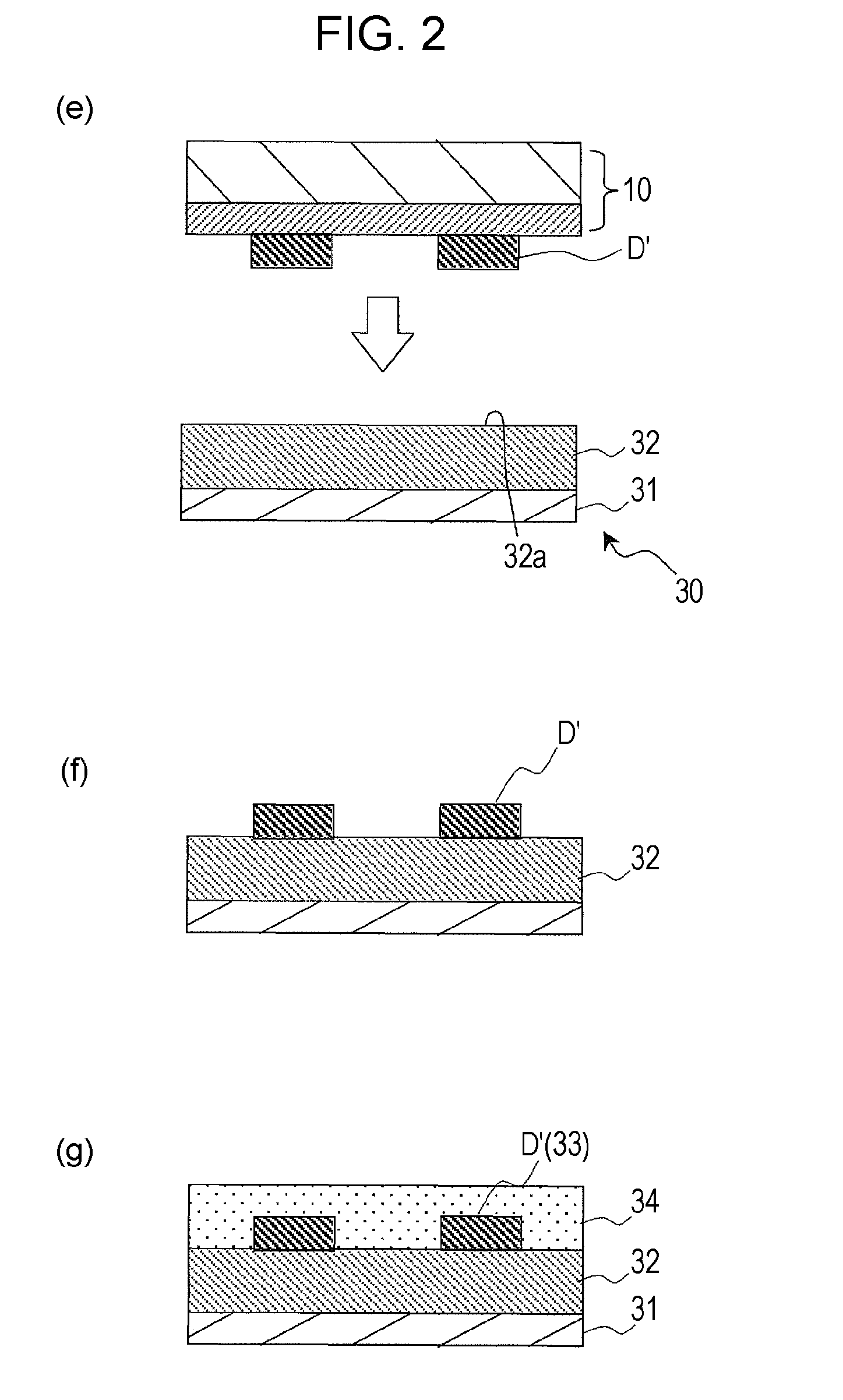
[0037]Furthermore, specific Examples of the present invention will now be described with reference to FIGS. 1 and 2 again.

examples 1 and 2

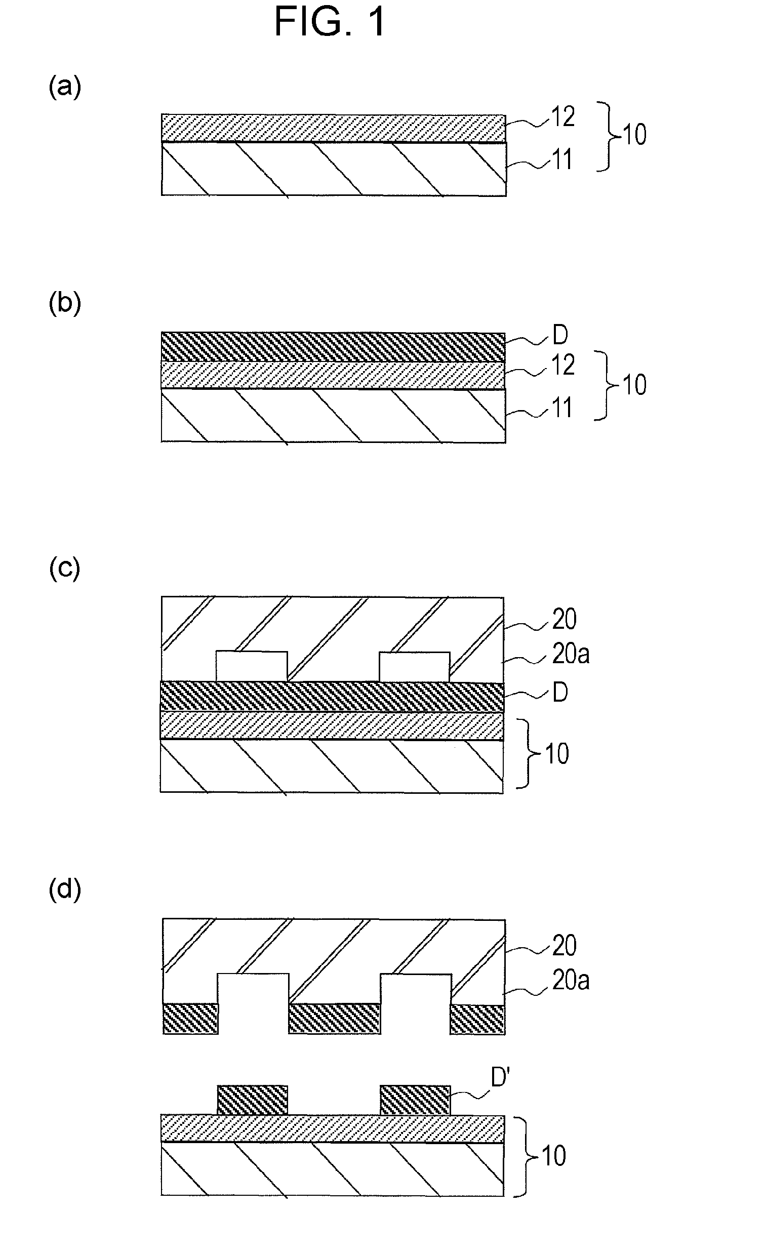
[0038]As in the embodiment described above, a first plate 10 (blanket) was prepared by applying a solution containing, as a main component, a resin material shown in Table 1 below onto a glass substrate 11 with a spin coater. Meanwhile, a solution containing, as a main component, a resin material shown in Table 1 below was applied onto a glass substrate to form a resin film. A projection-and-recess pattern was then formed on a surface side thereof by etching using an ordinary lithography technique so that a line-and-space (L / S) was 5 μm, thus forming a second plate 20.

TABLE 1First plateSecond plateLiquid compositionExample 1PolypropylenePolymethylXylenemethacrylateExample 2PolystyrenePolymethylTetralinmethacrylate(1,2,3,4-Tetrahydronaphthaline)ComparativePolystyrenePolymethylBenzyl alcoholExample 1methacrylateComparativePolypropylenePolymethylIsophoroneExample 2methacrylate(3,5,5-Trimethyl-2-cyclohexen-1-one)ComparativePolymethylPolystyreneTetralinExample 3methacrylate

[0039]Next, si...


PUM

PropertyMeasurementUnit
Timeaaaaaaaaaa
Viscosityaaaaaaaaaa
Electrical conductivityaaaaaaaaaa

Abstract

A method of forming a pattern and a method of producing an electronic element with which a fine and precise pattern is stably formed are provided. Each of the method of forming a pattern and the method of producing an electronic element includes a step of forming an electrically conductive film D by applying a liquid composition onto a first plate 10; a step of forming an electrically conductive pattern D′ on the first plate 10 by pressing a second plate 20 onto a surface side of the first plate 10, on which the electrically conductive film D is formed, to transfer an unwanted pattern of the electrically conductive film D to top faces of projections 20a of the second plate 20, thereby removing the unwanted pattern; and a step of transferring the electrically conductive pattern D′ by pressing the surface side of the first plate 10, on which the electrically conductive pattern D′ is formed, onto a surface of a transfer-receiving substrate, wherein when a surface tension of the surface of the first plate 10, onto which the liquid composition is applied, is represented by α, a dynamic surface tension of the liquid composition at 100 msec measured by a maximum bubble pressure method is represented by β, and a surface tension of the top faces of the projections 20a of the second plate 20 is represented by γ, the composition of the liquid composition or a material of the surface of the first plate 10 or the second plate 20 is set so as to satisfy γ>α≧β.

Description

TECHNICAL FIELD[0001]The present invention relates to a method of forming a pattern and a method of producing an electronic element. More specifically, the present invention relates to a method of forming an electrically conductive pattern and a method of producing an electronic element using the same.BACKGROUND ART[0002]Various methods have been studied in order to efficiently form a fine and precise pattern on a glass substrate, a plastic substrate, or the like at a low cost. For example, a printing method has been disclosed in which a resin to be printed is applied onto the entire surface of a first plate called a blanket, a surface of which is coated with silicone rubber having detachability, and a second plate having a projection-and-recess pattern on a surface side thereof is then pressed onto the surface side of the first plate, on which the resin is provided, to transfer an unwanted pattern of the resin to top faces of projections of the second plate, thereby removing the un...

Claims


Application Information

Patent Timeline
IPC IPC(8): B28B3/00
CPCH01L51/0022H01L51/0541H01L51/0545H05K2203/0108H05K3/046H05K3/207H01L51/102H10K71/611H10K10/464H10K10/82H10K10/466
Inventor FUKUDA, TOSHIONOMOTO, AKIHIRO
Owner SONY CORP
Why Eureka
Try Eureka