Through silicon via and method of fabricating same
- Summary
- Abstract
- Description
- Claims
- Application Information
AI Technical Summary
Benefits of technology
Problems solved by technology
Method used
Image

Examples
Embodiment Construction
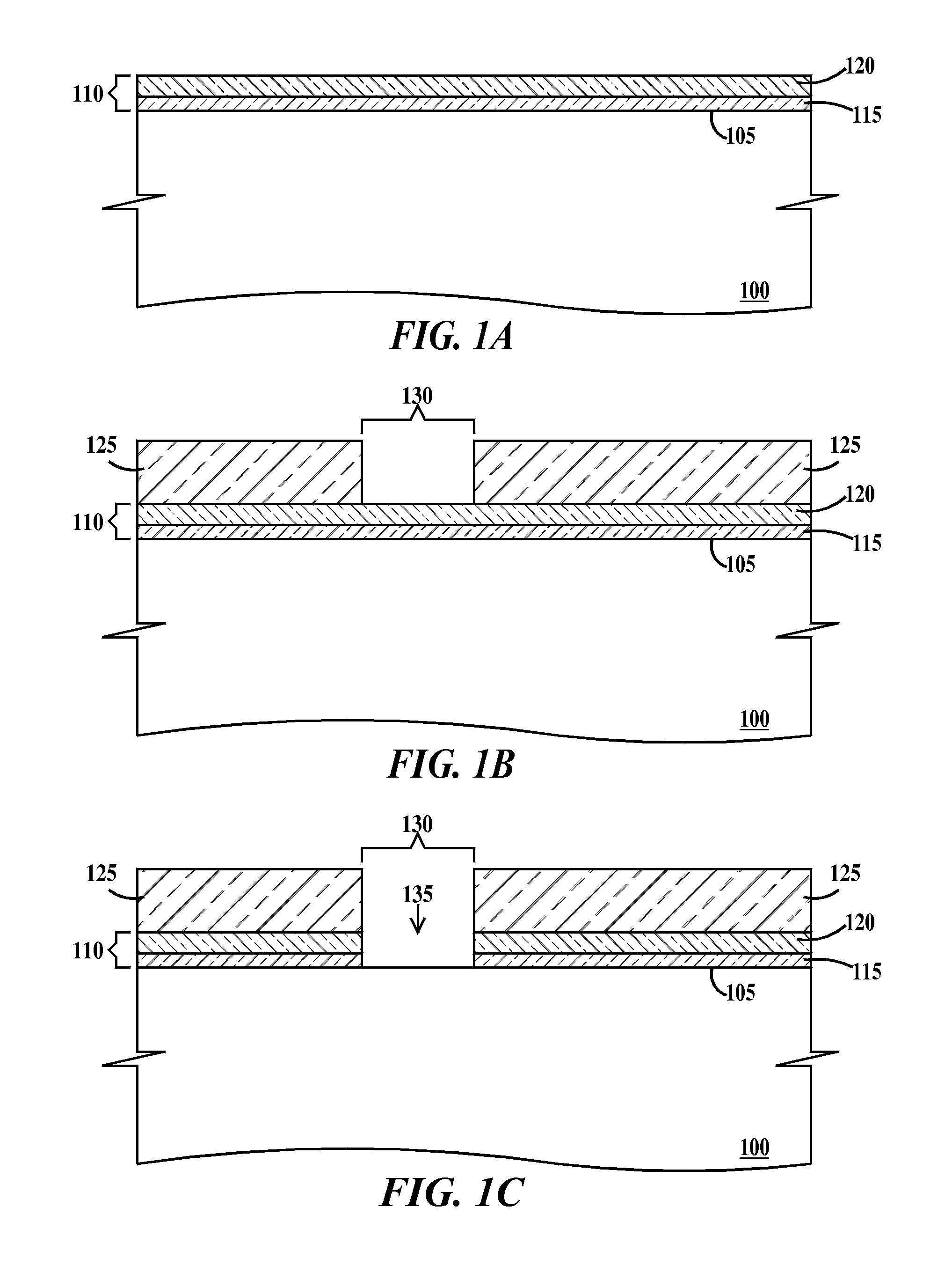
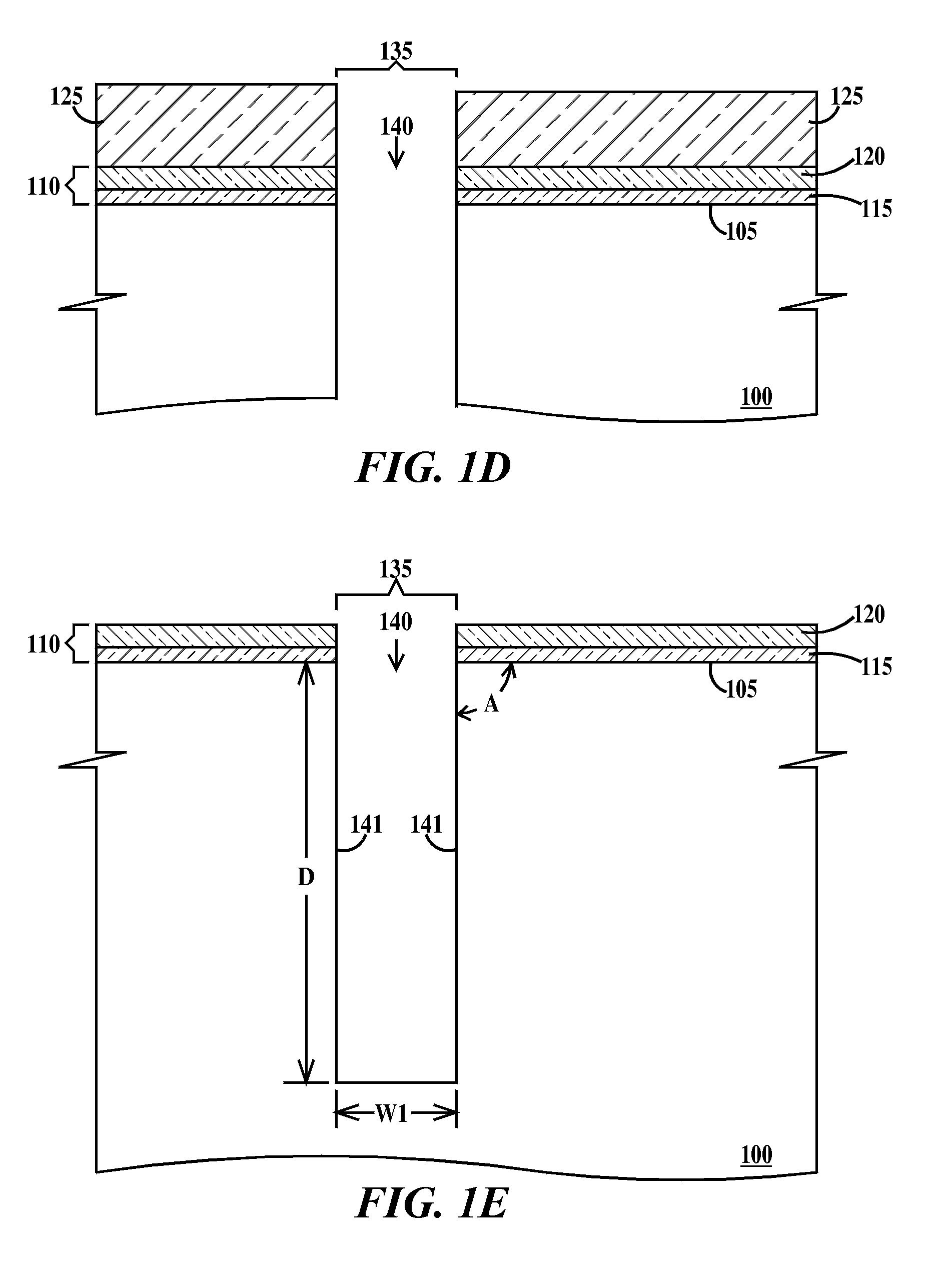
[0011]FIGS. 1A through 1M are cross-sectional views illustrating initial fabrication steps of a silicon through via according to embodiments of the present invention. In FIG. 1A, a single-crystal silicon substrate 100 has a top surface 105. In one example, substrate 100 has a crystal alignment relative to top surface 105. In one example, substrate 100 is doped P-type. Formed on top surface 105 of substrate 100 is a barrier layer 110. In one example, barrier layer 110 comprises two or more individual layers. In one example and as illustrated in FIG. 1A, barrier layer 110 consists of a first layer 115 on substrate 100 and second layer 120 on the first layer. In one example, first layer 115 is silicon dioxide and is between about 5 nm and about 20 nm thick and second layer 120 is silicon nitride and is between about 100 nm and about 30 nm thick. In one example, barrier layer 110 comprises one or more of a layer of silicon dioxide, a layer of silicon nitride and a layer of silicon carb...
PUM
 Abstract
Description
Claims
Application Information
 - R&D
- Intellectual Property
- Life Sciences
- Materials
- Tech Scout
- Unparalleled Data Quality
- Higher Quality Content
- 60% Fewer Hallucinations
Browse by: Latest US Patents, China's latest patents, Technical Efficacy Thesaurus, Application Domain, Technology Topic, Popular Technical Reports.
© 2025 PatSnap. All rights reserved.Legal|Privacy policy|Modern Slavery Act Transparency Statement|Sitemap|About US| Contact US: help@patsnap.com