
Ac-driven light emitting device having single active layer structure and manufacturing method thereof

a technology of light-emitting devices and active layers, which is applied in the direction of thermoelectric devices, organic semiconductor devices, luminescent compositions, etc., can solve problems such as device unstability operation, and achieve the effects of low manufacturing cost, simple structure and method, and easy reproduction

Inactive Publication Date: 2010-02-11
KOREA INST OF SCI & TECH
View PDF3 Cites 23 Cited by
  • Summary
  • Abstract
  • Description
  • Claims
  • Application Information

AI Technical Summary

Benefits of technology

[0021]Accordingly, a light emitting device and a manufacturing method thereof provides the following advantages.
[0024]3) Since a single active layer is used, a light emitting device can be manufactured using simple structure and method compared to an existing multi-layered structure formed by stacking a hole transport layer, an active layer, and an electron transport layer. Since the device can be easily reproduced at low manufacturing costs, advantageous process technology in an aspect of economical efficiency can be realized and used.

Problems solved by technology

In a device driven by a DC voltage, the life of the device may reduce or polymers may degrade due to an overcurrent, so that the device may unstably operate.

Method used


Image

  • Ac-driven light emitting device having single active layer structure and manufacturing method thereof
  • Ac-driven light emitting device having single active layer structure and manufacturing method thereof
  • Ac-driven light emitting device having single active layer structure and manufacturing method thereof

Examples


Embodiment Construction

[0036]Hereinafter reference will now be made in detail to various embodiments of the present invention, examples of which are illustrated in the accompanying drawings and described below. Terms used in the present invention are intended to explain a specific embodiment and not to limit the present invention. A singular expression includes a plural expression unless clearly expressed otherwise. Terms such as “include” and “have” in the present invention should be understood to designate existence of a characteristic, a number, a step, an operation, an element, a part, or a combination thereof on the specification, and not exclude one or more other characteristics, numbers, steps, operations, parts, or a combination thereof or possibility of addition.

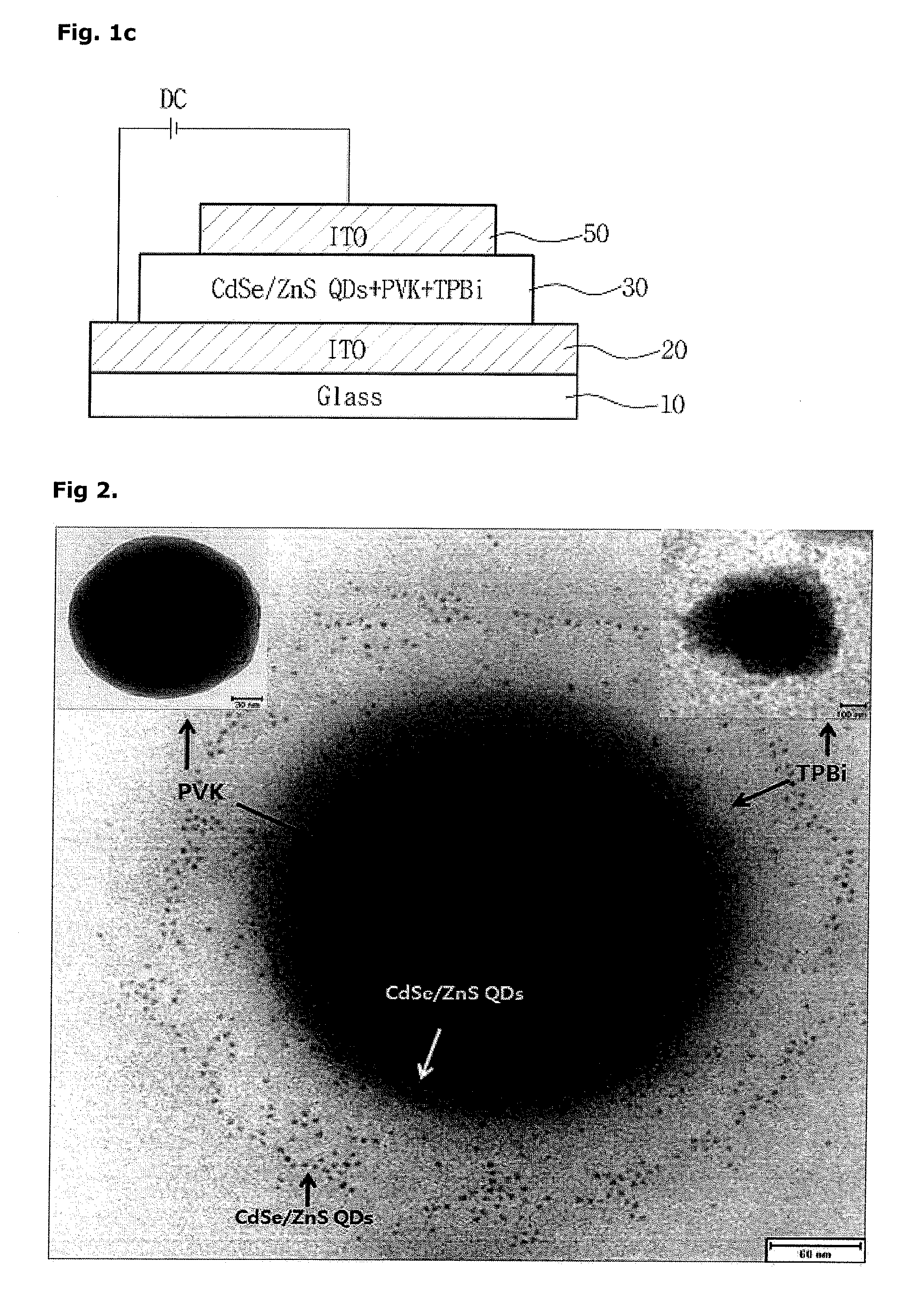
[0037]The present invention relates to an AC-driven LED having a single active layer of a consolidated core-shell structure, and a manufacturing method thereof.

[0038]Here, the active layer formed as a single layer has a p-i-n structure in...


PUM


Abstract

The present invention relates to an AC voltage-driven light emitting device having a single active layer of a core-shell structure (p-i-n structure) in which intrinsic semiconductor nanocrystals, exciton combination centers, are uniformly and isotropically distributed around p-type polymer particles, and n-type small molecular particles surround the semiconductor nanocrystals and p-type polymer, and a manufacturing method thereof. An active layer of a core-shell structure using a polymer-semiconductor nano hybrid in the light-emitting device has an inversion symmetry characteristic showing the same current-voltage characteristic during application of a voltage in a forward direction and a reverse direction. Therefore, due to this inversion symmetry characteristic, the light emitting can be driven by even an AC voltage. Also, since the device can be driven by an AC voltage, limitations of an existing DC voltage-driven organic light emitting diode, that is, destruction or a defect of the device by an overcurrent and generation of a dark spot by degradation of local constituent organic materials are solved.

Description

CROSS-REFERENCE TO RELATED APPLICATION[0001]This application claims under 35 U.S.C. §119(a) the benefit of Korean Patent Application No. 10-2008-0076710 filed on Aug. 5, 2008, the entire contents of which are incorporated herein by reference.BACKGROUND[0002](a) Technical Field[0003]The present invention relates to a light emitting device and a manufacturing method thereof. More particularly, the present invention relates to a light emitting device having a single active layer of a core-shell structure (p-i-n structure) in which intrinsic semiconductor nanocrystals, which serve as exciton combination centers, are uniformly and isotropically distributed around p-type polymer particles, and n-type small molecular particles surround the semiconductor nanocrystals and p-type polymer particles, and that can be driven even by an AC voltage, and a manufacturing method thereof.[0004](b) Background Art[0005]With rapid progress of electric and electronic technology, electric devices and electr...

Claims


Application Information

Patent Timeline
Patent Type & Authority Applications(United States)
IPC IPC(8): H01L51/54H01L51/56
CPCH01L51/5036H05B33/10H01L2251/564H01L2251/5369C09K11/883C09K11/02H10K50/125H10K2102/331H10K71/841
Inventor CHOI, WON KOOKPARK, DONG HEEIE, SANG YUBSON, DONG ICKCHOI, JI WON
Owner KOREA INST OF SCI & TECH
Learn More