Areal Active Pixel Image Sensor with Programmable Row-specific Gain for Hyper-Spectral Imaging

an image sensor and hyper-spectral imaging technology, applied in the field of electro-optical imaging devices, can solve the problems of substantial image signal distortion and undesirable in sensitive applications, and achieve the effect of minimizing the effect of dark leakage and high photoelectric gain

Inactive Publication Date: 2010-01-14
CMOS SENSOR
View PDF8 Cites 14 Cited by
  • Summary
  • Abstract
  • Description
  • Claims
  • Application Information

AI Technical Summary

Benefits of technology

[0024]In another embodiment, each APSjk further includes a photo-detector element switchably coupled to a serial connection of a resettable capacitive trans-impedance amplifier (CTIA) and a correlated double sampling (CDS) circuit. As a result, each APSjk produces the photoelectric signal PESjk with high photoelectric gain a

Problems solved by technology

While a conventional areal image sensor implements a uniform GOA for all its sensor pixels, such traditional implementation will result in substantial image signal distortion when applied to the

Method used


Image

  • Areal Active Pixel Image Sensor with Programmable Row-specific Gain for Hyper-Spectral Imaging
  • Areal Active Pixel Image Sensor with Programmable Row-specific Gain for Hyper-Spectral Imaging
  • Areal Active Pixel Image Sensor with Programmable Row-specific Gain for Hyper-Spectral Imaging

Examples


Embodiment Construction

[0048]The description above and below plus the drawings contained herein merely focus on one or more currently preferred embodiments of the present invention and also describe some exemplary optional features and / or alternative embodiments. The description and drawings are presented for the purpose of illustration and, as such, are not limitations of the present invention. Thus, those of ordinary skill in the art would readily recognize variations, modifications, and alternatives. Such variations, modifications and alternatives should be understood to be also within the scope of the present invention.

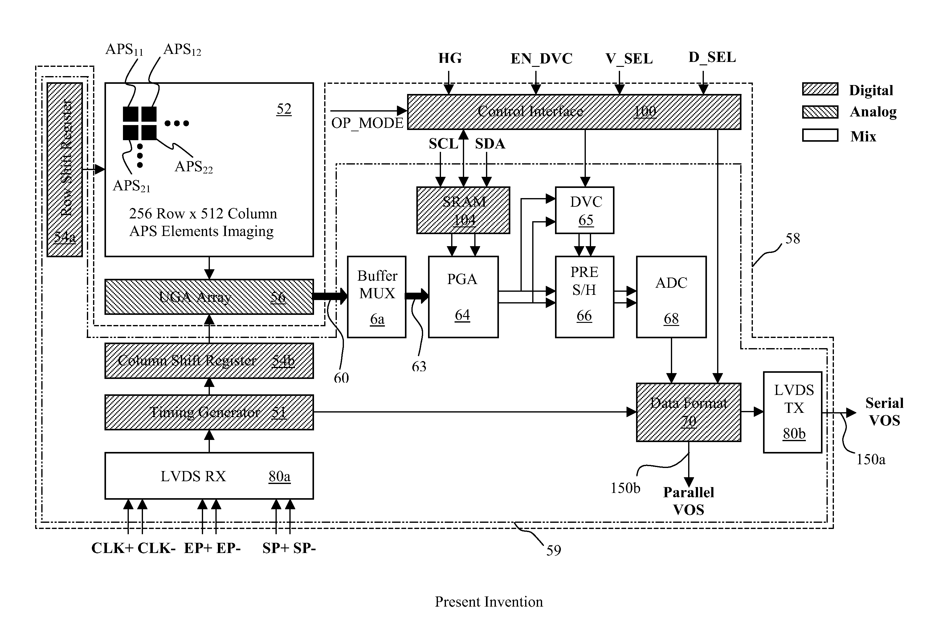
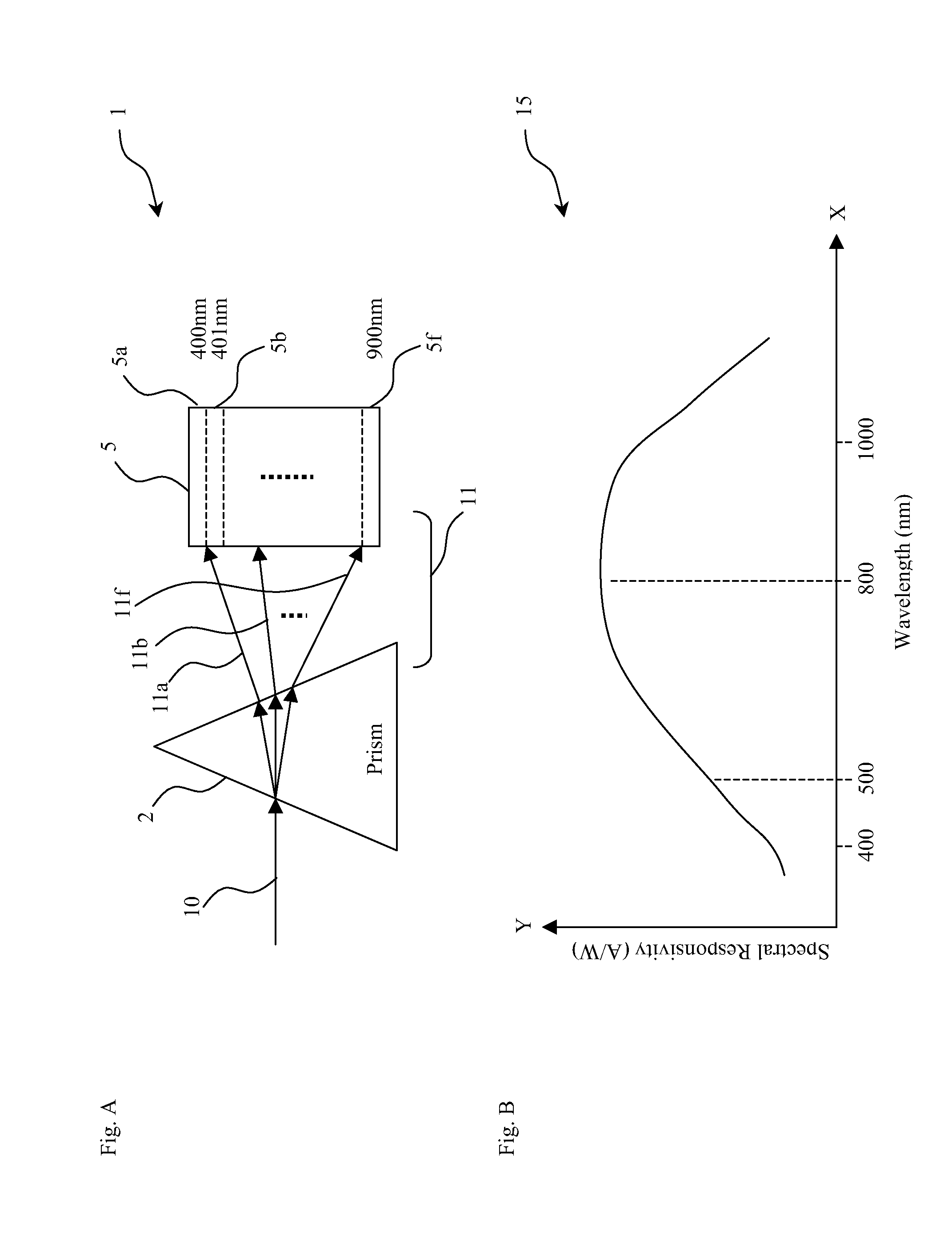
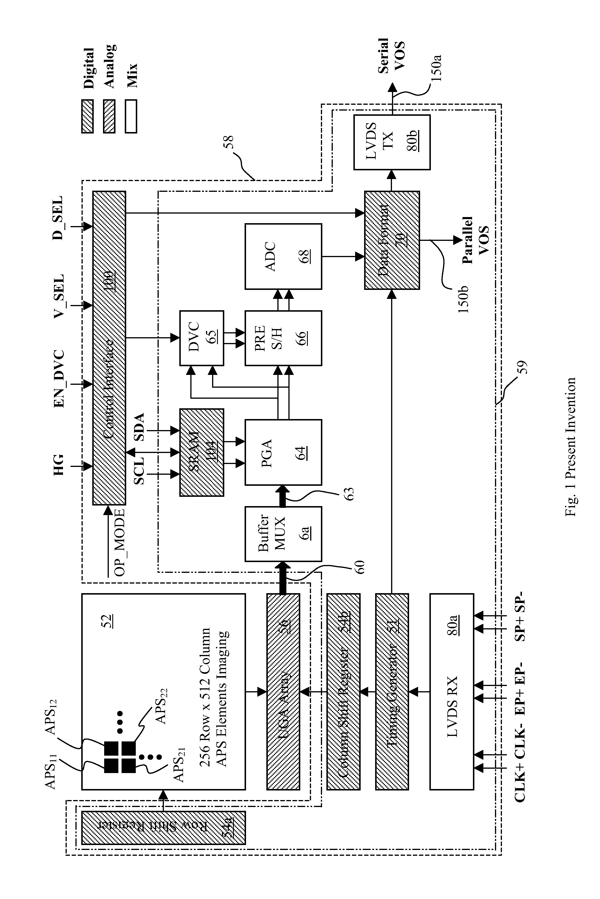
[0049]FIG. 1 illustrates an overall architecture of the present invention areal active pixel image sensor (AAPS) 50 with programmable row-specific gain. The AAPS 50 converts an incoming hyper-spectral light image 11 (see FIG. A) into a corresponding video output signal (VOS) that can be either a serial VOS 150a or a parallel VOS 150b by selection. The AAPS 50 is a mixed signal photoelec...


PUM


Abstract

An areal active pixel image sensor (AAPS) with programmable row-specific gain is disclosed for converting hyper-spectral light image into video output signal (VOS). The AAPS includes:
    • a) An areal active pixel sensor (APS) array each capable of photoelectrically converting and integrating an incident pixel light into a photoelectric signal through an integration time period TNT with a photoelectric signal gain GPE.
    • b) A video output signal conditioner (VOSC), coupled to the APS array, for multiplexing and amplifying the photoelectric signals into the VOS with an electric signal gain GEE.
    • c) The VOSC further programmably sets at least one of GPE and GEE to be row-specific.
Consequently, the AAPS exhibits an overall photoelectric signal gain of GOA=GPE×GEE that is row-specific and it can compensate for image signal distortion caused by non-uniform spectral response of the APS elements during hyper-spectral imaging.

Description

CROSS REFERENCE TO RELATED APPLICATIONS[0001]This application is related to the following U.S. patent application:[0002]Title: “A Multi-resolution Image Sensor Array with High Image Quality Pixel Readout Circuitry”, Inventors: Shengmin Lin, Weng-Lyang Wang. U.S. application Ser. No. 11 / 869,732 Attorney docket Number: CMOS003whose contents are incorporated herein by reference for any and all purpose and is referred to as U.S. Ser. No. 11 / 869,732.BACKGROUND OF THE INVENTION[0003]1. Field of the Invention[0004]The present invention relates to electronic imaging devices. More specifically, the invention provides an areal active pixel image sensor for hyper-spectral imaging.[0005]2. Description of Related Arts[0006]FIG. A illustrates a hyper-spectral imaging environment 1 wherein a prism 2 is used to separate a broadband light image 10 into a hyper-spectral light image 11 having numerous wavelength separated components: narrowband light image at λa 11a, narrowband light image at λb 11b, ...

Claims


Application Information

Patent Timeline
IPC IPC(8): H04N5/217H04N5/361H04N5/363H04N5/365H04N5/374H04N5/378
CPCH04N5/3745H04N5/361H04N25/63H04N25/77
Inventor WANG, WENG-LYANGLIN, SHENGMIN
Owner CMOS SENSOR
Why Eureka
Try Eureka