Semiconductor Nanowire Transistor

a technology of semiconductor nanowires and transistors, applied in transistors, nanotechnology, electric devices, etc., can solve the problems of weak thermal effects, small current on/off ratio, poor current control of transistors made of these materials, etc., and achieve the effects of reducing the impact ionization rate, improving the performance of the fet, and reducing the output conductan

Active Publication Date: 2009-12-31
QUNANO
View PDF4 Cites 25 Cited by
  • Summary
  • Abstract
  • Description
  • Claims
  • Application Information

AI Technical Summary

Benefits of technology

[0015]A further advantage of the invention is that the performance of the FET can be improved in that the heterostructure(s) make it possible to reduced output conductance via decreased impact ionization rate, improved current on / off ratios, reduced gate voltage swing via reduced drain induced barrier lowering, reduced contact resistance, and increased thermal stability.
[0016]Embodiments of the invention are defined in the dependent claims. Other objects, advantages and novel features of the invention will become apparent from the following

Problems solved by technology

However, transistors made of these materials often suffer from poor current control, small current on / off ratios, strong thermal effects, and a large output conductance related to the narrow band gap.
This is, with conventional technology, difficult, due to the large lattice mismatch between Si and III / V semiconductor materials.
These above mentioned effects limit the application areas of the III / V semiconductors devices and reduce the performance of analogue and digital applications. FIGS. 1a-c shows data for an InAs nanowire transistor, suffering from the above mentioned limitations: a) illustrates poor current control, b) the threshold control and c) the insufficient current on / off ratio.
This means that it is not possible to use heterostructures in the direction of the current path in the channel to improve the performance, as is done in vertical, for instance bipolar, transistors.
It is also difficult to fabricate heterostructures with narrow bandgap materials: in III / V semiconductors due to the lack of suitable lattice matched materials and problems with Sb-based compounds, and for Ge, the large lattice mismatch to Si and SiC.
Contacts to semiconductor devices is an area of special concern, as the contact resistance reduces speed and output power, but increases power consumption.

Method used


Image

  • Semiconductor Nanowire Transistor
  • Semiconductor Nanowire Transistor
  • Semiconductor Nanowire Transistor

Examples


first embodiment

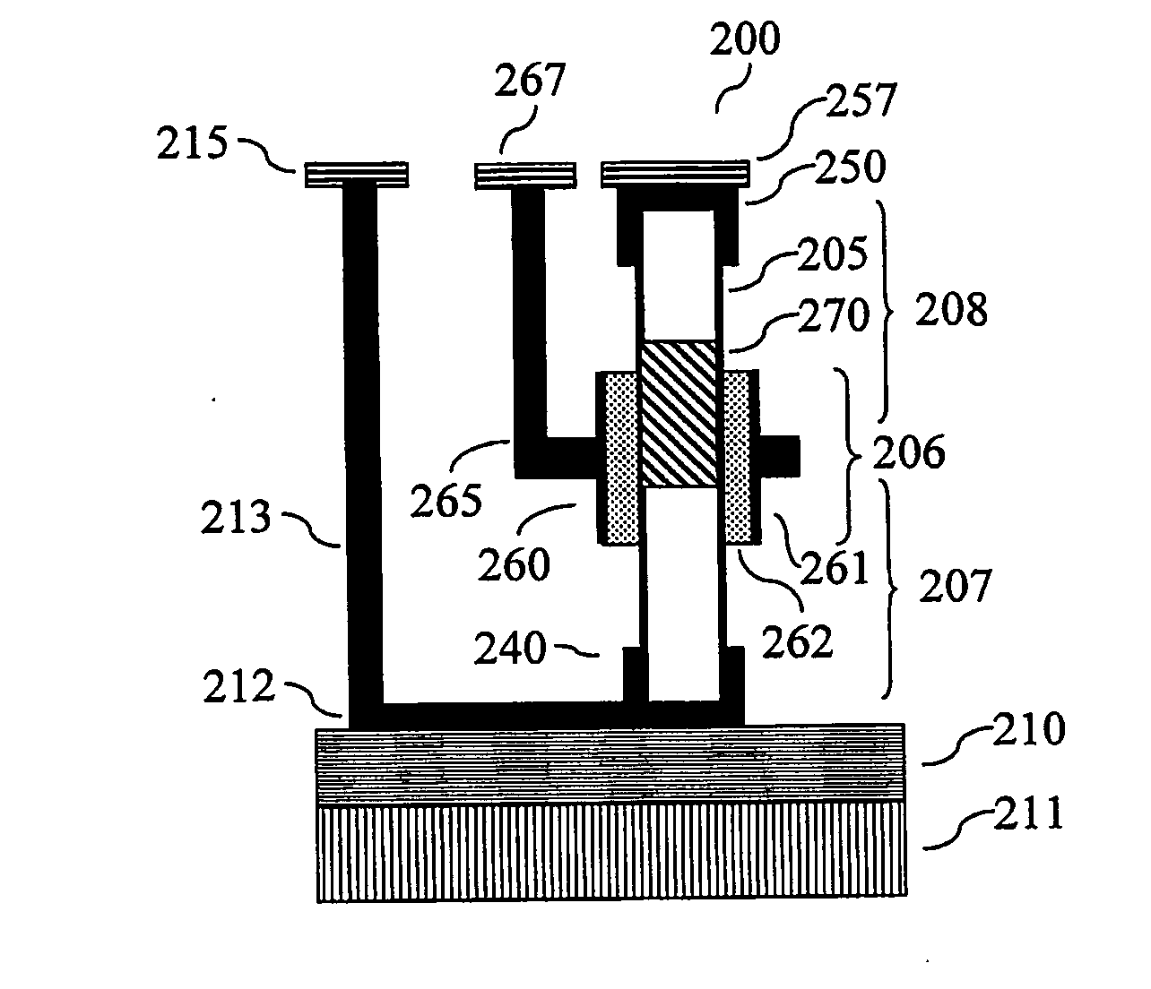
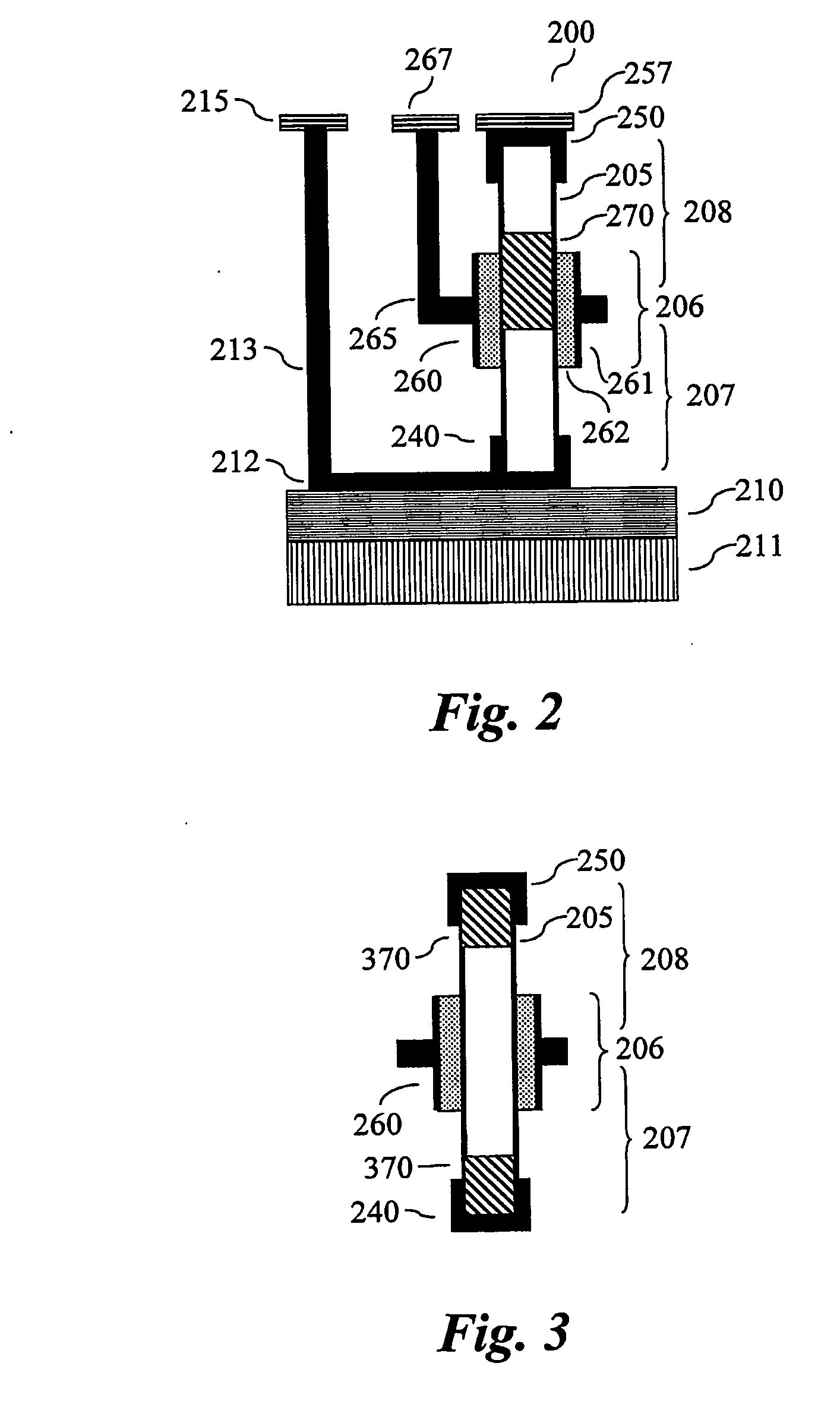
[0039]According to the invention one heterostructure 370 is provided in connection with either the drain 250 or source contact 240, or alternatively two heterostructures 370 are provided, one in connection with the drain contact 250, and one with the source contact 240, as illustrated in FIG. 3. The heterostructure(s) 370 consists of a segment of a semiconductor material of different constitution than the adjacent part or parts of the nanowire 205. The material of the heterostructure segment(s) 370 has a narrower band gap than the nanowire (like InAs, InSb, InGaAs or Ge, or alloys containing Al, Ga, In, As, P). Suitable band gap for the segment range from 200 to 500 MeV and segment lengths from 50 to 300 nm. Suitable materials include, but is not limited to InAs, InSb and Ge and combinations and alloys thereof The heterojunction can either be abrupt or graded. The narrow band gap reduces the specific contact resistance to the transistor and improves the performance. These segments a...

second embodiment

[0040]According to the invention a heterostructure 470 is provided in the high-field region between the gate and the drain, i.e. the gate-drain portion 208, and extends in the direction of the drain outside of the gate contact 260, as illustrated in FIG. 4. The heterostructure comprises a segment (length 50 to 500 nm) of a semiconductor material with wider band gap (ΔEg 100 meV to 2 eV) than the nanowire (like Si, SiGe, InP, GaAs, GaP, or alloys containing Al, Ga, In, As, P). Suitable materials include, but is not limited to InP, GaAs and AlAs and combinations and alloys thereof. The increased band gap reduces the impact ionization rate due to an increased band gap and / or a reduced electric field. The heterostructure may be either graded or abrupt.

third embodiment

[0041]According to the invention a heterostructure 570 is provided within the gate region 209, i.e. within the part of the nanowire enclosed by the wrap gate contact 260, as illustrated in FIG. 5. The heterostructure consists of a segment of a semiconductor material with wider band gap (ΔEc 100 to 300 meV) than the nanowire (like Si, SiGe, InP, GaAs, GaP, or alloys containing Al, Ga, In, As, P). Suitable materials for the segment include, but is not limited to InP, GaAs and AlAs and combinations and alloys thereof. The increased band gap enhances the maximum barrier height (˜Eg) that may be utilized for blocking the thermal current in the off-state of the transistor and increased the current on / off ratio. The heterojunction is sufficiently thick (>5 nm) to allow for diffusive-like transport (field assisted tunneling) across the interface. The heterojunction can either be abrupt or graded. The on-current still remains high due to tunneling and thermionic emission across the heterostr...


PUM


Abstract

A nanowire wrap-gate transistor is realised in a semiconductor material with a band gap narrower than Si. The strain relaxation in the nanowires allows the transistor to be placed on a large variety of substrates and heterostructures to be incorporated in the device. Various types of heterostructures should be introduced in the transistor to reduce the output conductance via reduced impact ionization rate, increase the current on / off ratio, reduction of the sub-threshold slope, reduction of transistor contact resistance and improved thermal stability. The parasitic capacitances should be minimized by the use of semi-insulating substrates and the use of cross-bar geometry between the source and drain access regions. The transistor may find applications in digital high frequency and low power circuits as well as in analogue high frequency circuits.

Description

TECHNICAL FIELD[0001]The present invention relates to a transistor device of nanoscale dimensions. In particular the invention relates to a wrap gate field effect transistor with a nanowire or nanowires as an essential member in the current path.BACKGROUND[0002]Semiconductor materials with narrow band gap, hereinafter referred to as III / V semiconductors, such as InAs and InSb, have high mobilities, high saturated carrier velocities and low contact resistances. This makes the materials good candidates for high-speed and low-power electronics, and over the recent years the interest in using these materials in a large variety of semiconductor devices has shown a significant increase. However, transistors made of these materials often suffer from poor current control, small current on / off ratios, strong thermal effects, and a large output conductance related to the narrow band gap. In addition, structures of III / V semiconductors should preferably, in order to be commercially interesting...

Claims


Application Information

Patent Timeline
Patent Type & Authority Applications(United States)
IPC IPC(8): H01L29/12
CPCB82Y10/00H01L29/0665H01L29/0673H01L29/775H01L29/068H01L29/165H01L29/205H01L29/0676
Inventor WERNERSSON, LARS-ERIKBRYLLERT, TOMASLIND, ERIKSAMUELSON, LARS
Owner QUNANO
Why Eureka
Try Eureka