
Image-pickup device and display apparatus

Active Publication Date: 2009-12-17
JAPAN DISPLAY WEST
View PDF18 Cites 16 Cited by
  • Summary
  • Abstract
  • Description
  • Claims
  • Application Information

AI Technical Summary

Benefits of technology

[0011]According to the present invention, because an amplification function depends on the source follower circuit, the analog output can be realized as in the case of a CCD or a CMOS image sensor, which is a general image-pickup device. The speed of image-pickup processing can be increased, and the number of gradations of the image-pickup result can be increased. Thus, by using the characteristics of the analog output that allows half tones to be excellently represented, a touch panel function, a scanner function, or the like can be realized. Furthermore, it can be considered that the image-pickup devices are applied as dimmer sensors for a backlight in a liquid-crystal display apparatus. Moreover, the amplifying thin-film transistor performs the analog output, thereby realizing the amplification function. Thus, for example, when TFT-type photosensors are used as the photoelectric conversion elements, respective constituent elements of the image-pickup devices can be manufactured using a process the same as that of typical TFTs. For example, the respective constituent elements can be disposed in display pixels of a liquid-crystal display apparatus. In other words, the image-pickup devices are very suitable for realization of integration with a display function. In addition, for example, when the image-pickup devices are embedded in the display pixels of the liquid-crystal apparatus, the image-pickup devices can be disposed so that a great decrease in aperture ratio is reduced, and can be easily disposed in a matrix for the respective display pixels. Thus, for example, multipoint recognition that was difficult to be realized in touch panels in the prior art can be realized, and a probability that the image-pickup devices will serve as key devices of a new user interface that does not exist in the prior art can be expected.

Problems solved by technology

When the above-described image-pickup devices of a display-function-integrated type are realized using a commonly known low-temperature polysilicon technique, it is considered that it is difficult to obtain accurate output values because it is impossible to disregard attenuation of signals that is caused by parasitic capacitances in panels.

Method used


Image

  • Image-pickup device and display apparatus
  • Image-pickup device and display apparatus
  • Image-pickup device and display apparatus

Examples


first embodiment

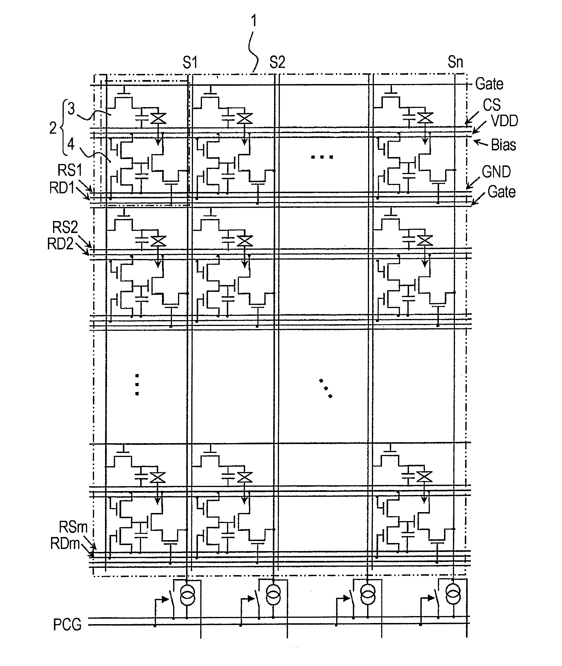
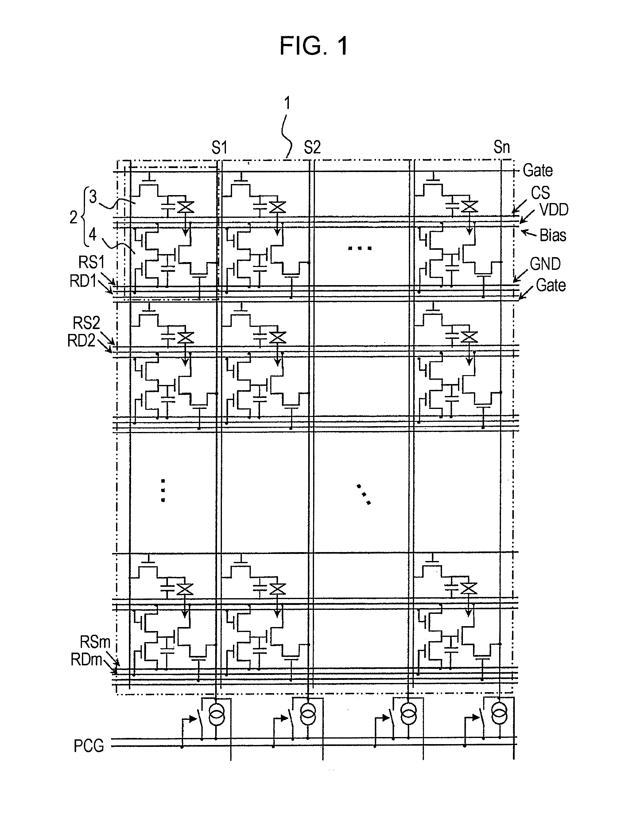
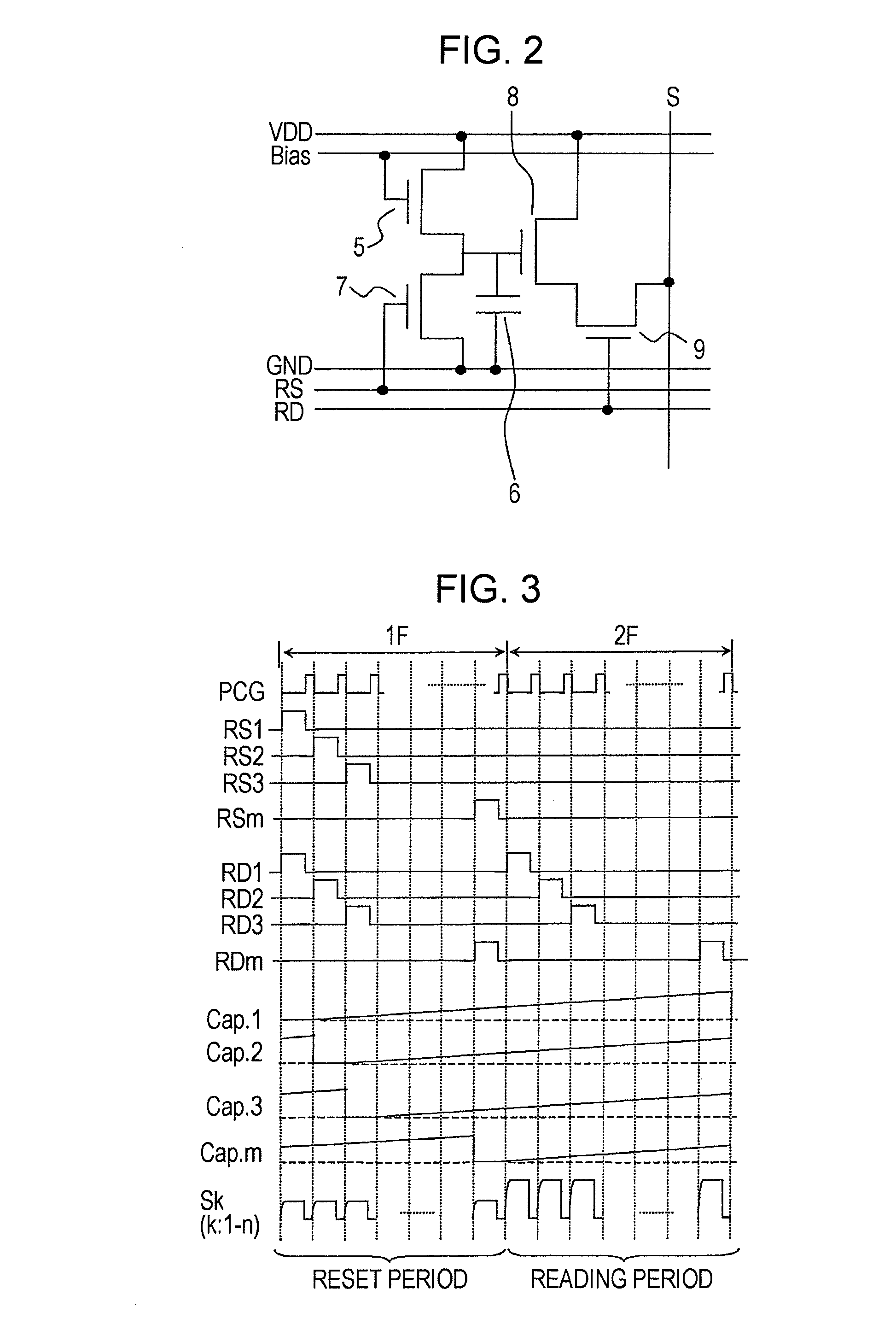
[0023]First, a first embodiment of the present invention is described. FIG. 1 is a circuit diagram showing an example of a schematic configuration of the display apparatus according to the present invention. FIG. 2 is a circuit diagram showing the first embodiment of the image-pickup device that is the main portion of the display apparatus.

[0024]First, the entire display apparatus is described. The display apparatus that is described in the embodiment is a display apparatus in which a display function and an image-pickup function are integrated. In a broad classification, as shown in FIG. 1, the display apparatus is configured by including an image-display-region section 1, a backlight or a frontlight (however, not illustrated) that serves as a light source, and a driver circuit section (however, not illustrated) for performing drive control for the image-display-region section 1.

[0025]The image-display-region section 1 is configured of a plurality of pixel units 2 that are disposed...

second embodiment

[0058]Next, a second embodiment of the present invention will be described. However, herein, only the difference between the second embodiment and the above-described first embodiment is described.

[0059]In the first embodiment, the reset TFT 7 is provided as reset means. Accordingly, when the image-pickup element portion 4 is disposed in each of the respective pixel units 2, which are disposed in the matrix, a decrease in the aperture ratio of the display element portion 3 only by a portion corresponding to the provided reset TFT 7 may occur. In contrast, although the gate voltage of the sensor TFT 5 is set to be equal to or lower than a threshold when the sensor TFT 5 is used as a photoelectric conversion element, it is known that, if the setting of the gate voltage is appropriately changed, the sensor TFT 5 can operate as a normal transistor. Thus, in an image-pickup element portion 4 that is to be described as an example in the embodiment, the gate voltage of the sensor TFT 5 is ...


PUM


Abstract

An image-pickup device includes a photoelectric conversion element 5 that converts light into electric charge, a capacitor 6 that stores electric charge which the photoelectric conversion element 5 has obtained by conversion, reset means 7 for discharging the electric charge in the capacitor 6, and an amplifying thin-film transistor 8 that receives, amplifies, and outputs the electric charge stored in the capacitor 6. In addition, the image-pickup device is configured so that the amplifying thin-film transistor 8 forms a source follower circuit.

Description

TECHNICAL FIELD[0001]The present invention relates to an image-pickup device including photoelectric conversion elements, and a display apparatus.BACKGROUND ART[0002]While, in general, photoelectric conversion elements, such as CCD (Charge Coupled Devices) sensors and CMOS (Complementary Metal Oxide Semiconductor) sensors, have been known as image-pickup devices that pick up images, recently, it has been proposed that thin-film transistors (hereinafter, “Thin Film Transistor” is abbreviated as “TFT”) are caused to function as photoelectric conversion elements in combination with capacitors or the like. As one example of such image-pickup devices, for example, there are image-pickup devices that include liquid-crystal display elements, TFTs that function as photoelectric conversion elements, and so forth for respective pixels disposed in a matrix, and that also include a backlight or frontlight which serves as a light source. The image-pickup devices are configured so as to be capabl...

Claims


Application Information

Patent Timeline
IPC IPC(8): H04N5/335G09G3/36G02F1/133G06F3/041G06F3/042G09G3/20H04N1/028H04N5/222H04N5/369H04N5/374H04N5/3745
CPCG02F1/13338G02F2001/13312G09G2300/0465G09G3/3648G06F3/0412G06F3/042G02F1/13312
Inventor MATSUI, MASAFUMINAKAJIMA, YOSHIHARUTERANISHI, YASUYUKI
Owner JAPAN DISPLAY WEST
Learn More