System and Method for Thermal Optimized Chip Stacking

a technology of thermal optimization and stacking chips, applied in the direction of electrical equipment, semiconductor devices, semiconductor/solid-state device details, etc., can solve the problems of large number of chips creating problems with cooling, affecting the efficiency of the system, and the power dissipation density of most functions implemented in silicon is not uniform, so as to reduce the impact of hot spots and uniform power density , the effect of uniform power density

Inactive Publication Date: 2009-12-10
IBM CORP
View PDF9 Cites 3 Cited by
  • Summary
  • Abstract
  • Description
  • Claims
  • Application Information

AI Technical Summary

Benefits of technology

[0010]The present invention is generally directed at providing a low cost solution for dissipating heat generated within chip stacks.
[0012]Using the flexibility of thru-silicon via technology, a method for creating a more uniform power density by distributing the hot spots of an individual layer in a chip stack is created. This reduces the impact of the hot spots on adjacent layers within the stack, and thus reduces the magnitude between the average temperature on the die and the hot spots.
[0013]The present invention is advantageous over previous solutions because the chips used on each of the layers may be identical, therefore creating no additional production costs.

Problems solved by technology

One challenge of stacking chips is thermal management.
Specifically, chip stacks with a greater number of chips create problems with cooling.
If such heat is not dissipated out of the chip stack, technical issues may occur.
Getting the “heat” out of the die in the middle of the stack is generally recognized as a large challenge.
Further complicating this challenge is the fact that most functions implemented in silicon do not have a uniform power dissipation density.
This may create additional heating effects and cause the hot spots to be even more pronounced relative to the rest of the silicon surface area in the stack.
However, wire bonding is not practical to allow the rotation of the bus interface along with the die rotation and is not very effective in large chip stacks because the bonds get long, degrading signal and power integrity.

Method used


Image

  • System and Method for Thermal Optimized Chip Stacking
  • System and Method for Thermal Optimized Chip Stacking
  • System and Method for Thermal Optimized Chip Stacking

Examples


Embodiment Construction

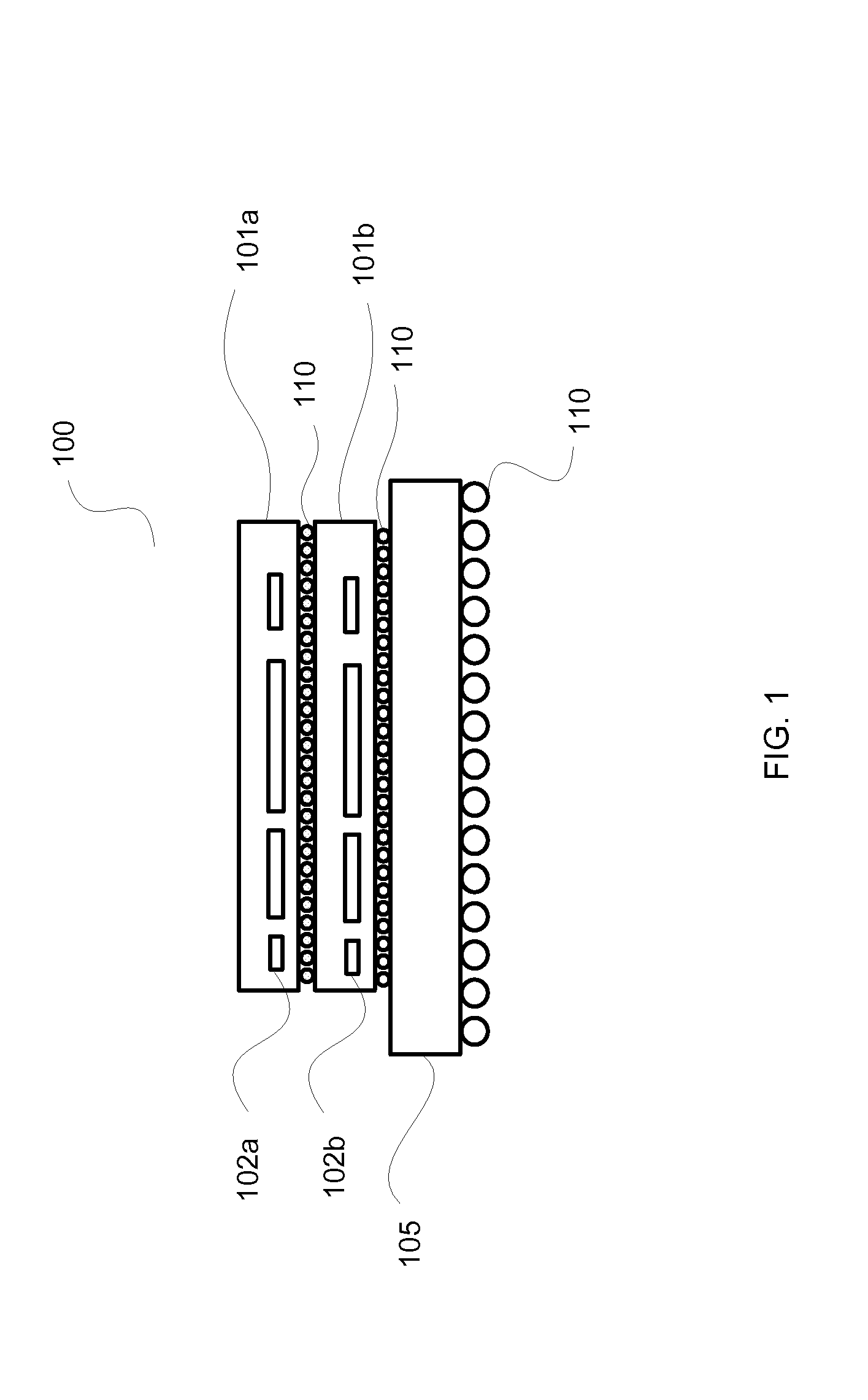
[0020]FIG. 1 illustrates a side view of an exemplary chip stack 100. Chip stack 100 includes chips 101a and 101b, package 105, and C4 connectors 110. In this exemplary figure, chips 101a and 101b sit directly above and below each other. Each of the processor cores in respective chips 101a and 101b create hot spots 102a and 102b that also sit directly above and below each other. These hotter areas, hot spots 102a and 102b, may heat each other causing an even greater temperature increase over the average in this region.

[0021]Those of ordinary skill in the art will recognize that chip stack 100 may include more than the exemplified two chips. In addition, it will be understood that each of the chips include other components such as memory 103a and 103b, memory controls 104a and 104b, and other logic components. Furthermore, it will be understood that hot spots 102a and 102b may be created by elements in the chip other than the processor cores.

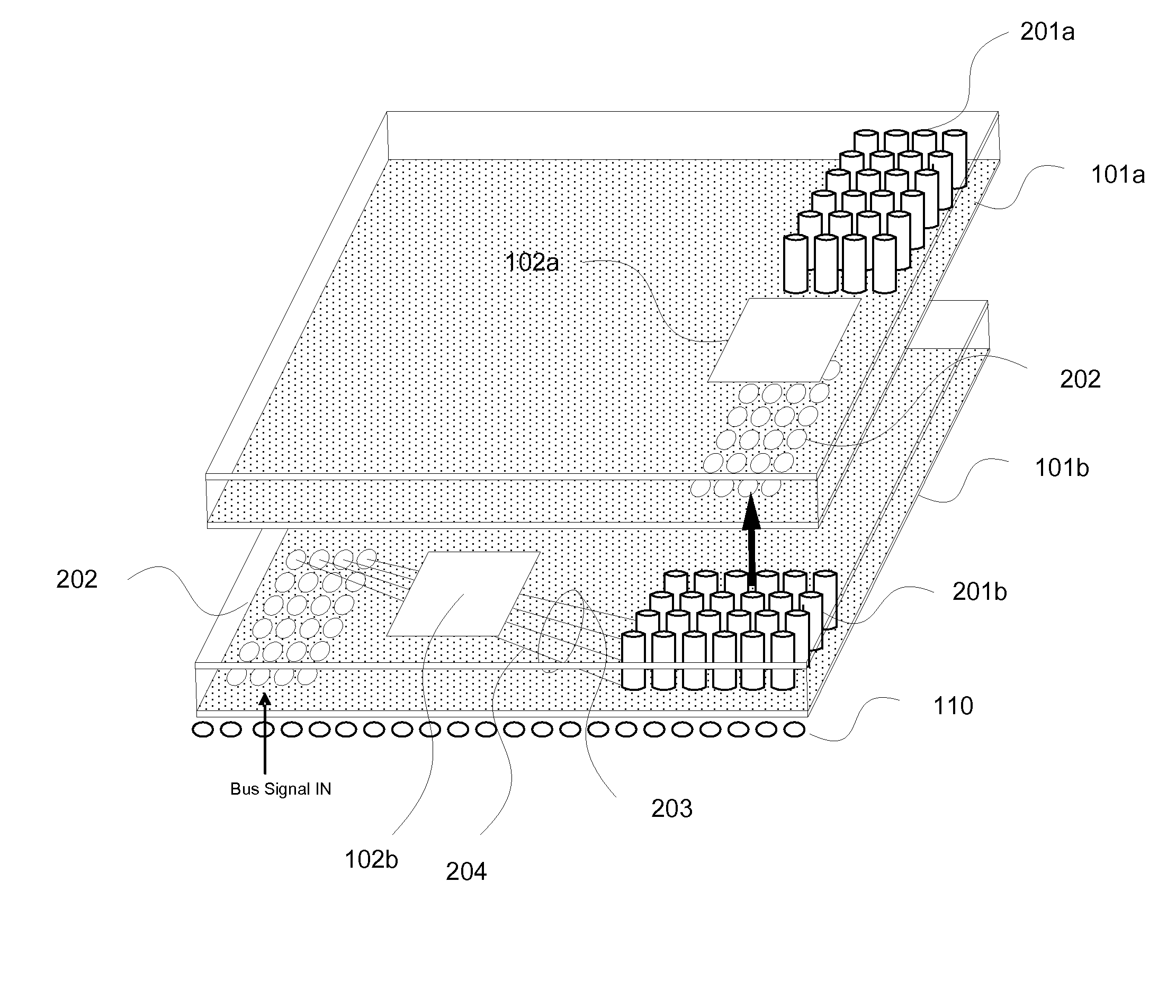
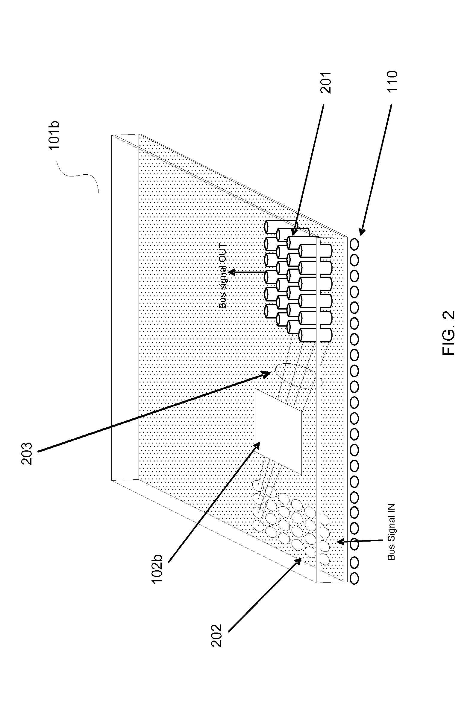
[0022]FIG. 2 illustrates a perspective view...


PUM


Abstract

A method for thermal optimization comprising the steps of stacking a first chip layer and a second chip layer wherein the second chip layer is rotated in relation to the first chip layer wherein a first hot spot on the first chip layer and a second hot spot on the second chip layer are not spatially aligned; routing a signal input through the first chip layer from a first chip pad on the first chip layer to a first silicon via so as to form a physical input to output twist and a first signal output; and routing the first signal output from the first chip layer through a second chip layer from a second chip pad on the second chip layer to a second silicon via so as to form a second signal output.

Description

BACKGROUND OF THE INVENTION[0001]1. Field of the Invention[0002]The present invention relates to a system and method for stacking integrated circuits or chips. Specifically, the present invention relates to a system and method for thermal optimization in stacked chips.[0003]2. Description of Background[0004]Integrated circuit or chip manufacturers use chip stacks in order to build more powerful devices. For example, packaged integrated circuit devices, i.e., chips, including, for example, microprocessors, memory devices are stacked together, e.g., back-to-front or back-to-back. Chip stacks are beneficial because they allow more compact circuit arrangements and, therefore, more efficient use of space, e.g., on circuit boards. The advent of thru-silicon via on three-dimensional chip-stacking as a packaging approach has opened up opportunities for creating more compact functions than ever before. Stacks of chips have been demonstrated with greater than ten chips in the stack.[0005]Thos...

Claims


Application Information

Patent Timeline
Patent Type & Authority Applications(United States)
IPC IPC(8): H01L21/58
CPCH01L23/50H01L24/16H01L25/0657H01L2224/0557H01L2224/16H01L2225/06513H01L2225/06517H01L2924/0002H01L2225/06589H01L2924/14H01L2924/15311H01L2224/0401H01L2224/05552H01L2224/023H01L2924/0001
Inventor BARTLEY, GERALD K.BECKER, DARRYL J.DAHLEN, PAUL E.GERMANN, PHILIP R.MAKI, ANDREW B.MAXSON, MARK O.
Owner IBM CORP
Why Eureka
Try Eureka