
IC device having low resistance TSV comprising ground connection

Active Publication Date: 2009-11-12
TEXAS INSTR INC
View PDF5 Cites 114 Cited by
  • Summary
  • Abstract
  • Description
  • Claims
  • Application Information

AI Technical Summary

Benefits of technology

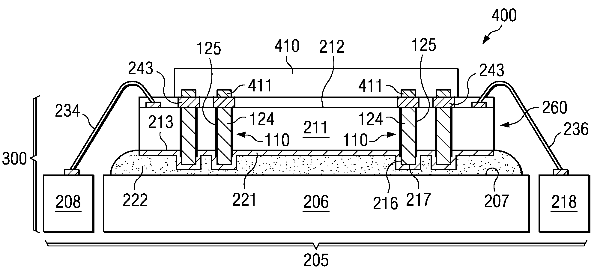
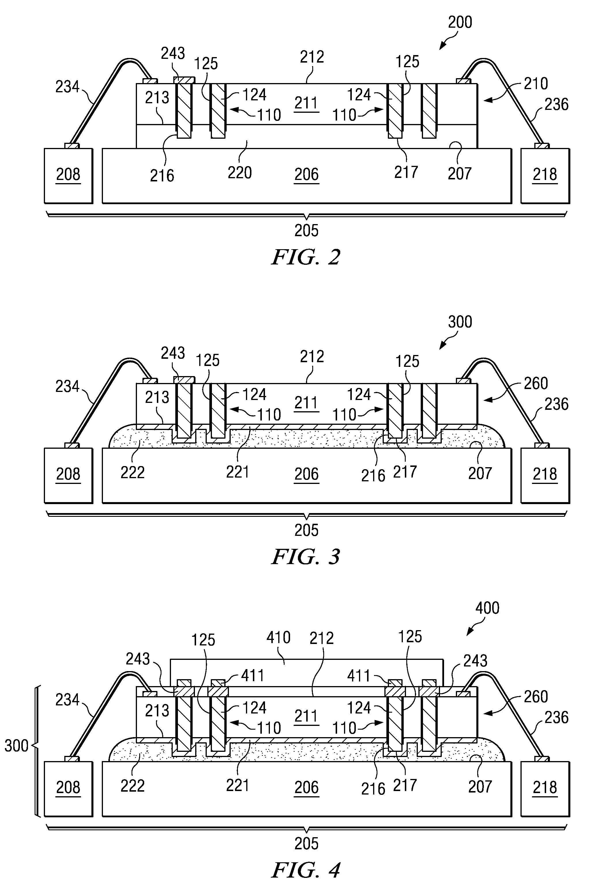
[0008]By combining a metal layer on the bottom surface of the IC and the protruding integral TSV tips along with ground connection enhancement region comprising interconnect mediums described herein, the electrical resistance can be further reduced. The minimum nominal resistance between the protruding integral TSV tips and a package substrate (e.g., die pad) provided by the embodiments of the invention is estimated as being at least an order of magnitude up to several orders of magnitude lower as compared to the ACF arrangement described in the background above, making embodiments of the invention particularly well suited for improving the performance of analog ICs, such as for RF ICs including power amplifiers.

Problems solved by technology

Although the ACF arrangement reduces the electrical resistance between the TSV tips and the package substrate somewhat, the reduction is limited because the ACF particles are generally 3-5 μm in size (and are thus significantly smaller than the typical distance between the TSV tip(s) and a package substrate) and the particle loading is such that the statistical probability of trapping enough (if any) particles beneath the TSV tip diameter to make a low resistance electrical joint is low.
Accordingly, the minimum nominal resistance between the TSV tips and the package substrate (e.g., die pad) provided by the ACF arrangement is still generally too high for proper performance of certain analog ICs, in particular for certain RF ICs, such as power amplifiers.
The Present Inventors have recognized that using the ACF arrangement described above generally does not reduce the minimum nominal electrical resistance between the TSV tips and the die pad or other package substrate sufficiently for a low resistance ground for proper performance of certain ICs, such as RF ICs (e.g., power amplifiers).
A selectivity lower than about 10 will generally cause excessive loss of the dielectric liner.
Lower selectivity below about 2:1 can cause excessive loss of the electrically conductive filler material.
Lower selectivity can cause excessive loss of the electrically conductive filler material.

Method used


Image

  • IC device having low resistance TSV comprising ground connection
  • IC device having low resistance TSV comprising ground connection
  • IC device having low resistance TSV comprising ground connection

Examples


Embodiment Construction

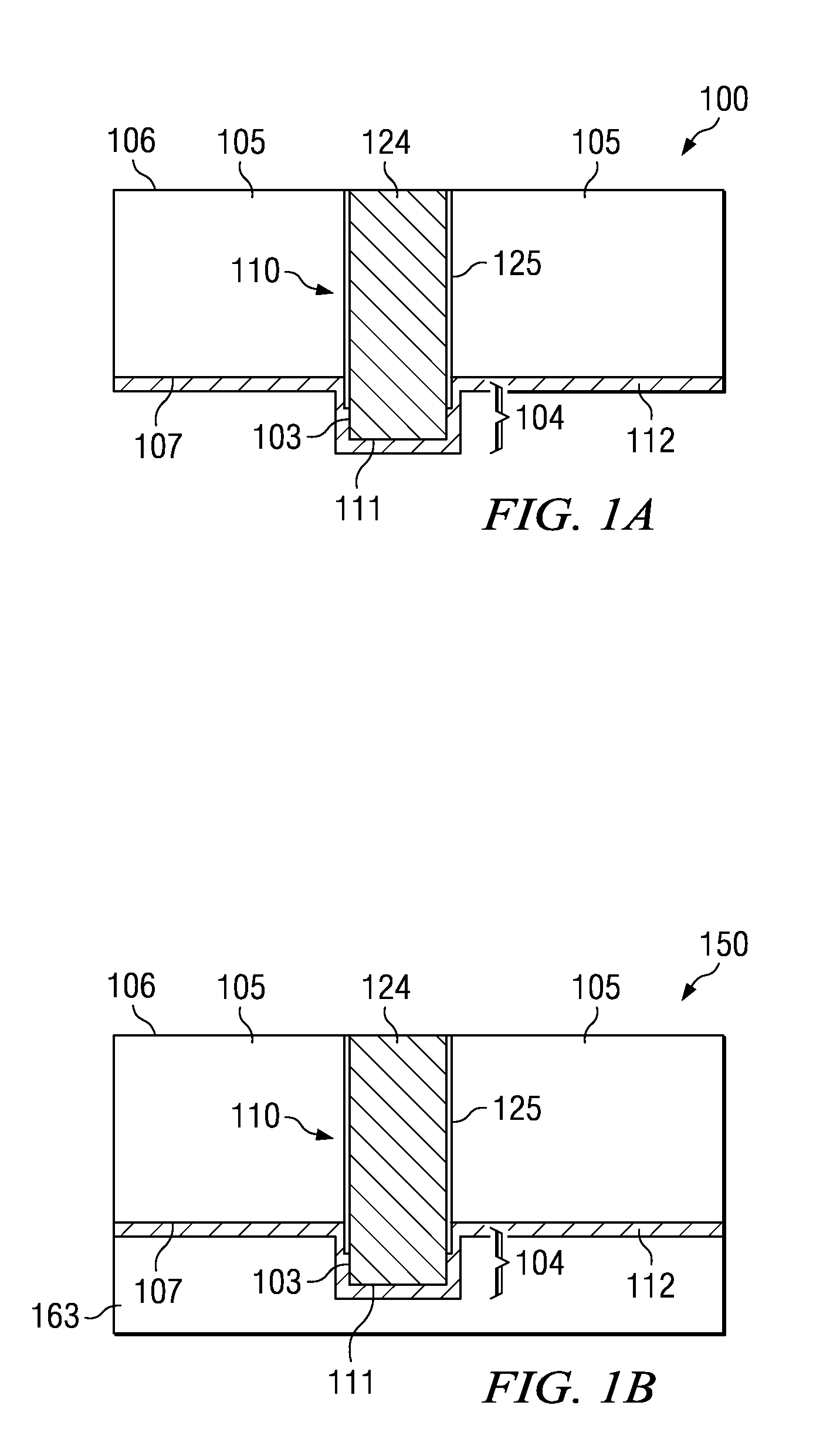
[0018]The present invention is described with reference to the attached figures, wherein like reference numerals are used throughout the figures to designate similar or equivalent elements. The figures are not drawn to scale and they are provided merely to illustrate the instant invention. Several aspects of the invention are described below with reference to example applications for illustration. It should be understood that numerous specific details, relationships, and methods are set forth to provide a full understanding of the invention. One having ordinary skill in the relevant art, however, will readily recognize that the invention can be practiced without one or more of the specific details or with other methods. In other instances, well-known structures or operations are not shown in detail to avoid obscuring the invention. The present invention is not limited by the illustrated ordering of acts or events, as some acts may occur in different orders and / or concurrently with o...


PUM


Abstract

A semiconductor device includes an integrated circuit (IC) die including a substrate, and at least one through substrate via (TSV) that extends through the substrate to a protruding integral tip that includes sidewalls and a distal end. The protruding integral tip has a tip height between 1 and 50 μm. A metal layer is on the bottom surface of the IC die, and the sidewalls and the distal end of the protruding integral tips. A semiconductor device can include an IC die that includes TSVs and a package substrate such as a lead-frame, where the IC die includes a metal layer and an electrically conductive die attach adhesive layer, such as a solder filled polymer wherein the solder is arranged in an electrically interconnected network, between the metal layer and the die pad of the lead-frame.

Description

CROSS REFERENCE TO RELATED APPLICATIONS[0001]This application claims the benefit of Provisional Application Ser. No. 61 / 052,471 entitled “METHODS OF MAKING IMPROVED ELECTRICAL CONNECTION IN IC CHIPS USING THROUGH Si VIAS”, filed May 12, 2008, which is herein incorporated by reference in its entirety.FIELD OF THE INVENTION[0002]Embodiments of the present invention relate to integrated circuit (IC) devices having through substrate vias (TSVs).BACKGROUND[0003]As known in the art, TSVs which are also referred to as through-wafer vias (TWVs), are vertical electrical connections that pass from the frontside surface of a wafer or IC die (e.g., contact level or one of the metal levels) completely through to the backside surface. As a result, electrical paths through the device can be significantly shortened relative to conventional wire bonding technology, leading to significantly faster device operation and smaller footprints because the interconnect is within the footprint of the IC die a...

Claims


Application Information

Patent Timeline
IPC IPC(8): H01L23/538H01L23/522H01L23/495H01L21/768H01L21/60
CPCH01L2924/04953H01L2924/078H01L2924/14H01L2924/30107H01L23/481H01L23/49513H01L23/49575H01L24/16H01L24/30H01L24/33H01L24/48H01L24/73H01L25/0657H01L2224/0557H01L2224/16145H01L2224/2919H01L2224/293H01L2224/32145H01L2224/32225H01L2224/48091H01L2224/48247H01L2224/73204H01L2224/73207H01L2224/73265H01L2225/0651H01L2225/06513H01L2225/06541H01L2924/01005H01L2924/01013H01L2924/01015H01L2924/01029H01L2924/01038H01L2924/01047H01L2924/0105H01L2924/01073H01L2924/01074H01L2924/01078H01L2924/01079H01L2924/01082H01L2924/01006H01L2924/01033H01L2924/01072H01L2924/014H01L2224/29111H01L2924/0132H01L2224/16245H01L2224/32245H01L2224/73257H01L2224/2929H01L2224/29339H01L2224/0401H01L2924/1461H01L2924/00014H01L2924/0002H01L2924/00H01L2924/01083H01L2924/0665H01L2224/05552H01L24/05H01L2224/05647H01L2224/45099H01L2224/45015H01L2924/207H01L2924/013
Inventor DUNNE, RAJIVMORRISON, GARY P.CHAUHAN, SATYENDRA S.MURTUZA, MASOODBONIFIELD, THOMAS D.
Owner TEXAS INSTR INC
Learn More