Semiconductor Device and Method for Fabricating the Same

a technology of semiconductor devices and semiconductor devices, applied in semiconductor devices, semiconductor/solid-state device details, electrical apparatus, etc., can solve the problems of reducing increasing resistance, etc., to prevent degradation of the operating speed of semiconductor devices, increase resistance, and improve yield and reliability of semiconductor devices

Inactive Publication Date: 2009-11-05
SK HYNIX INC
View PDF3 Cites 5 Cited by
  • Summary
  • Abstract
  • Description
  • Claims
  • Application Information

AI Technical Summary

Benefits of technology

[0013]Various embodiments of the present invention are directed at providing a method for fabricating a semiconductor device that may include forming a metal word line additionally over a vertical transistor to obtain a multi-layered structure, thereby preventing degradation of the operating speed of the semiconductor device due to an increase of resistance of a damascene word line that connects a surrounding gate of a vertical transistor. As a result, the yield and reliability of the semiconductor device can be improved.

Problems solved by technology

The increase of resistance lowers the operating speed of the semiconductor device.

Method used


Image

  • Semiconductor Device and Method for Fabricating the Same
  • Semiconductor Device and Method for Fabricating the Same
  • Semiconductor Device and Method for Fabricating the Same

Examples


Embodiment Construction

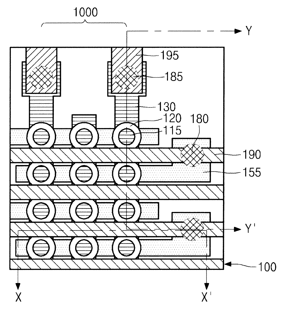
[0026]FIG. 4 is a diagram illustrating a semiconductor device according to an embodiment of the present invention.

[0027]The semiconductor device of FIG. 4 includes a plurality of word lines 155 configured to electrically connect surrounding gates of a vertical transistor in a given number unit and a second word line 190 arranged parallel to the first word lines over the first word lines and configured to supply a gate voltage to the first word lines 155. The second word line 190 is connected to the first word lines 155, which are electrically connected to the second word line 190 through a contact plug 180. The second word line 190 includes a metal line having an excellent conductivity. The second word line 190 receives a gate power from a peripheral circuit region and provides the gate power to the first word lines 155.

[0028]As can be seen, the gate voltage from the peripheral circuit region is not directly applied to the damascene. Instead, the gate voltage is supplied to the firs...


PUM


Abstract

A method for fabricating a semiconductor device includes forming a metal word line additionally over a vertical transistor to obtain a multi-layered structure, thereby preventing degradation of the operating speed of the semiconductor device by preventing an increase of resistance of a damascene word line that connects a surrounding gate of a vertical transistor. As a result, the yield and reliability of the semiconductor device can be improved.

Description

[0001]The priority benefit of Korean patent application number 10-2008-0041442, filed on May 2, 2008, is hereby claimed and the disclosure thereof is incorporated herein by reference in its entirety.BACKGROUND OF THE INVENTION[0002]Semiconductor devices such as DRAM have required including many transistors in a limited region so as to improve integration. Accordingly, a vertical transistor as a element included in high integrated memory cell generally having an area of 4 F2 has been suggested. The vertical transistor has a surrounding gate structure that surrounds a vertical channel.[0003]In order to form the surrounding gate in area 4 F2 area, a channel region is selectively isotropic-etched so that the channel region is formed to be thinner than the source / drain regions, thereby obtaining excellent device characteristics. As a result, the vertical transistor can use a limited area effectively. Furthermore, the vertical transistor has been spotlighted in various fields with DRAMs b...

Claims


Application Information

Patent Timeline
IPC IPC(8): H01L23/535H01L21/768
CPCH01L27/10876H01L29/7827H01L27/10891H10B12/053H10B12/488H10B12/395H10B12/0383
Inventor CHUNG, SUNG WOONGHWANG, SANG MINKIM, HYUN JUNG
Owner SK HYNIX INC
Why Eureka
Try Eureka