
Light-emitting device as well as lighting apparatus and display apparatus using the same

a technology of light-emitting devices and lighting apparatus, which is applied in the direction of lasers, semiconductor lasers, lighting and heating apparatus, etc., can solve the problems of practically undesirable use of light-emitting devices, interference fringes in outgoing light, and laser beams that interfere with each other, so as to reduce the return light and weaken the coherence of laser light

Inactive Publication Date: 2009-10-08
SHARP KK
View PDF7 Cites 10 Cited by
  • Summary
  • Abstract
  • Description
  • Claims
  • Application Information

AI Technical Summary

Benefits of technology

[0016]In the light of the aforementioned problem, it is an object of the present invention to provide a light-emitting device, a lighting apparatus and a display apparatus in which the laser light of low coherence is produced even in a light-emitting device using a power circuit not having a high-frequency superposition function, and the color rendering index of emitting light is improved.
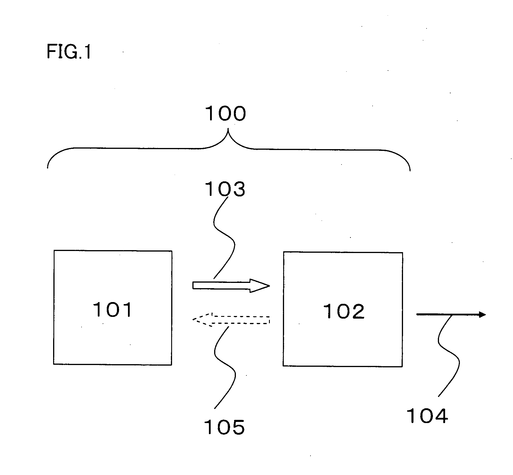
[0019]Here, the self-oscillation (semiconductor) laser element used in the present invention is a laser element in which an outgoing laser light blinks in a short cycle by the element alone. Structure of the self-oscillation semiconductor laser element is not particularly limited insofar as it causes self-oscillation, and for example, a structure having a region referred to as a saturable absorbing layer (S.A.) in the vicinity of an active layer can be recited. When a saturable absorbing layer is provided in the vicinity of an active layer, the saturable absorbing layer serves to conduct absorption and release of the laser light generating in the active layer, so that the outgoing laser light blinks in a short cycle. In other words, it is possible to obtain the same effect as that obtainable by superposing high frequency current on the single mode laser, by the element alone in the self-oscillation laser element. As a result, it is possible to reduce the return light and weaken the coherence of the laser light.
[0028]According to the present invention, since the coherence of the laser light can be weakened in the light-emitting device using the semiconductor laser element and the phosphor, it is possible to suppress the phenomenon undesirable for the light-emitting device such as interference fringe or light unevenness of the outgoing light. In addition, it is possible to obtain a light-emitting device capable of maintaining the outgoing light having a higher output and better stability than a conventional one.

Problems solved by technology

However, in a conventional light-emitting device using a semiconductor laser element, the following problems exist.
When the array-type semiconductor laser element is used, since the laser light outgoes from a plurality of light-emitting points, the plurality of laser beams interfere with each other and interference fringe arises in the outgoing light.
It is practically undesirable to use a light-emitting device using such a semiconductor laser element, as a lighting apparatus or a display apparatus, because unevenness in light emission is caused.
Such a light is refereed to as “a return light” and is a cause of making a laser oscillation operation, or an optical output of the semiconductor laser element unstable.
When such a light-emitting device is used as a lighting apparatus or a display apparatus, it may result in unevenness in light emission and is not practically desirable.

Method used


Image

  • Light-emitting device as well as lighting apparatus and display apparatus using the same
  • Light-emitting device as well as lighting apparatus and display apparatus using the same
  • Light-emitting device as well as lighting apparatus and display apparatus using the same

Examples


example 1

[0056]FIG. 3 is a schematic section view of the light-emitting device according to Example 1.

[0057]An array-type self-oscillation semiconductor laser element 301 is mounted on a block 303 that is formed integrally with a stem 302. The array-type self-oscillation semiconductor laser element is connected with a pin 305 that is formed integrally with the stem via a wire 304, and the array-type self-oscillation semiconductor laser element can be energized by supplying electric power to the pin from outside of the light-emitting device. The array-type self-oscillation semiconductor laser element is arranged inside a space 307 that is hermetically sealed by a cap 306. However, the cap is provided with a transmission window 308 made of a glass, and as a result, a laser light 309 emitted from the array-type self-oscillation semiconductor laser element is released outside the hermetically sealed space through the transmission window. Further, a phosphor 310 is arranged outside the cap, and t...

example 2

[0136]FIG. 11 is a section view of the self-oscillation semiconductor laser element according to Example 2 of the present invention, viewed from the stripe direction.

[0137]The nitride semiconductor laser element has a structure having a P type saturable absorbing layer, and includes an N electrode 1110, an n-GaN substrate 1111, an n-GaN layer 1112, an n-InGaN crack preventive layer 1113, an S.A. system 1114, an n-GaN guide layer 1115, an n-InGaN active layer 1116, a p-AlGaN carrier block layer 1117, a p-GaN guide layer 1118, a p-AlGaN clad layer 1119, a p-GaN contact layer 1120, an insulation film 1121, and a P electrode 1122, from the side of the substrate.

[0138]FIG. 12 shows the S.A. system of Example 2. From the side of the substrate, a first C.E. of n-AlGaN 1201, a second C.E. of InGaN 1202, an S.A. of InGaN 1203, a third C.E. of InGaN 1204, and a fourth C.E. of n-AlGaN 1205 are provided.

[0139]Example 2 has an identical form to Example 1 except that the laser element shown in FI...

example 3

[0151]FIG. 13 is a schematic section view showing the light-emitting device according to Example 3 of the present invention.

[0152]An array-type self-oscillation semiconductor laser element 1301 is mounted on a block 1303 that is formed integrally with a stem 1302. The array-type self-oscillation semiconductor laser element is connected with a pin 1305 that is formed integrally with the stem via a wire 1304, and the array-type self-oscillation semiconductor laser element can be energized by supplying electric power to the pin from outside of the light-emitting device. The array-type self-oscillation semiconductor laser element is arranged inside a space 1307 that is hermetically sealed by a cap 1306. However, the cap is provided with a transmission window 1308 made of a glass, and as a result, a laser light 1309 emitted from the array-type self-oscillation semiconductor laser element is released outside the hermetically sealed space through the transmission window. Further, a phospho...


PUM


Abstract

A light-emitting device including a semiconductor laser element having at least a substrate, a first conductive type clad layer, an active layer, and a second conductive type clad layer in this order; and a phosphor absorbing a laser light emitted from the semiconductor laser element and radiating fluorescence, wherein the semiconductor laser element is a self-oscillation laser element.

Description

[0001]This nonprovisional application is based on Japanese Patent Application No. 2008-064604 filed on Mar. 13, 2008 with the Japan Patent Office, the entire contents of which are hereby incorporated by reference.BACKGROUND OF THE INVENTION[0002]1. Field of the Invention[0003]The present invention relates to a light-emitting device having a semiconductor laser element and a phosphor, and more specifically, to a light-emitting device usable as a lighting apparatus or a display apparatus.[0004]2. Description of the Background Art[0005]In recent years, light-emitting devices using a semiconductor light-emitting device and a phosphor have been developed as substitutes for conventional light-emitting devices such as an incandescent lamp and a fluorescent lamp. As one example of the semiconductor light-emitting device, a light-emitting diode including a light-emitting layer of group III-V compound semiconductor can be recited, and light-emitting diodes emitting a light in red, green, as w...

Claims


Application Information

Patent Timeline
Patent Type & Authority Applications(United States)
IPC IPC(8): F21V9/16
CPCB82Y20/00H01S5/005H01S5/0202H01S5/02288H01S5/028H01S2301/02H01S5/0658H01S5/2215H01S5/34326H01S5/4031H01S5/0425H01L2224/48091H01L2224/48247H01S5/04252H01S2301/176H01S5/02253H01S5/34333H01S5/02257H01S5/0087H01S5/02251H01S2304/04H01S5/02469H01L2924/00014
Inventor YAMASAKI, YUKIOKISHIMOTO, KATSUHIKO
Owner SHARP KK
Learn More