
Semiconductor device having vertical channel transistor and method for fabricating the same

a technology of vertical channel transistor and semiconductor device, which is applied in the direction of semiconductor devices, electrical devices, transistors, etc., can solve the problems of difficult to realize a semiconductor device with high-speed performance, and difficulty in downscaling memory devices having linewidths of 40 nm or less, so as to reduce the resistance of a word line and high-speed performance

Inactive Publication Date: 2009-09-24
SK HYNIX INC
View PDF7 Cites 36 Cited by
  • Summary
  • Abstract
  • Description
  • Claims
  • Application Information

AI Technical Summary

Benefits of technology

[0011]Embodiments are directed to providing a semiconductor device with a vertical channel transistor, which can realize high-speed performance by reducing a sheet resistance of a word line, and a method for fabricating the semiconductor device.

Problems solved by technology

However, it is very difficult to realize a downscaled memory device having a linewidth of 40 nm or less using a typical planar or recessed gate transistor having 8F2 or 6F2 cell architecture, (the capital letter ‘F’ represents a minimum feature size).
Accordingly, the sheet resistance of the word line is greatly increased due to the polysilicon layer having a high sheet resistance, which makes it difficult to realize a semiconductor device with high-speed performance.

Method used


Image

  • Semiconductor device having vertical channel transistor and method for fabricating the same
  • Semiconductor device having vertical channel transistor and method for fabricating the same
  • Semiconductor device having vertical channel transistor and method for fabricating the same

Examples


Embodiment Construction

[0029]In the figures, the dimensions of layers and regions are exaggerated for clarity of illustration. It will also be understood that when a layer is referred to as being “on / under” another layer or substrate, it can be directly on / under the other layer or substrate, or intervening layers may also be present. Like reference numerals refer to like elements throughout the drawings. In addition, changes to the English characters of the reference numerals of layers refer to a partial deformation of the layers by an etch process or a polishing process.

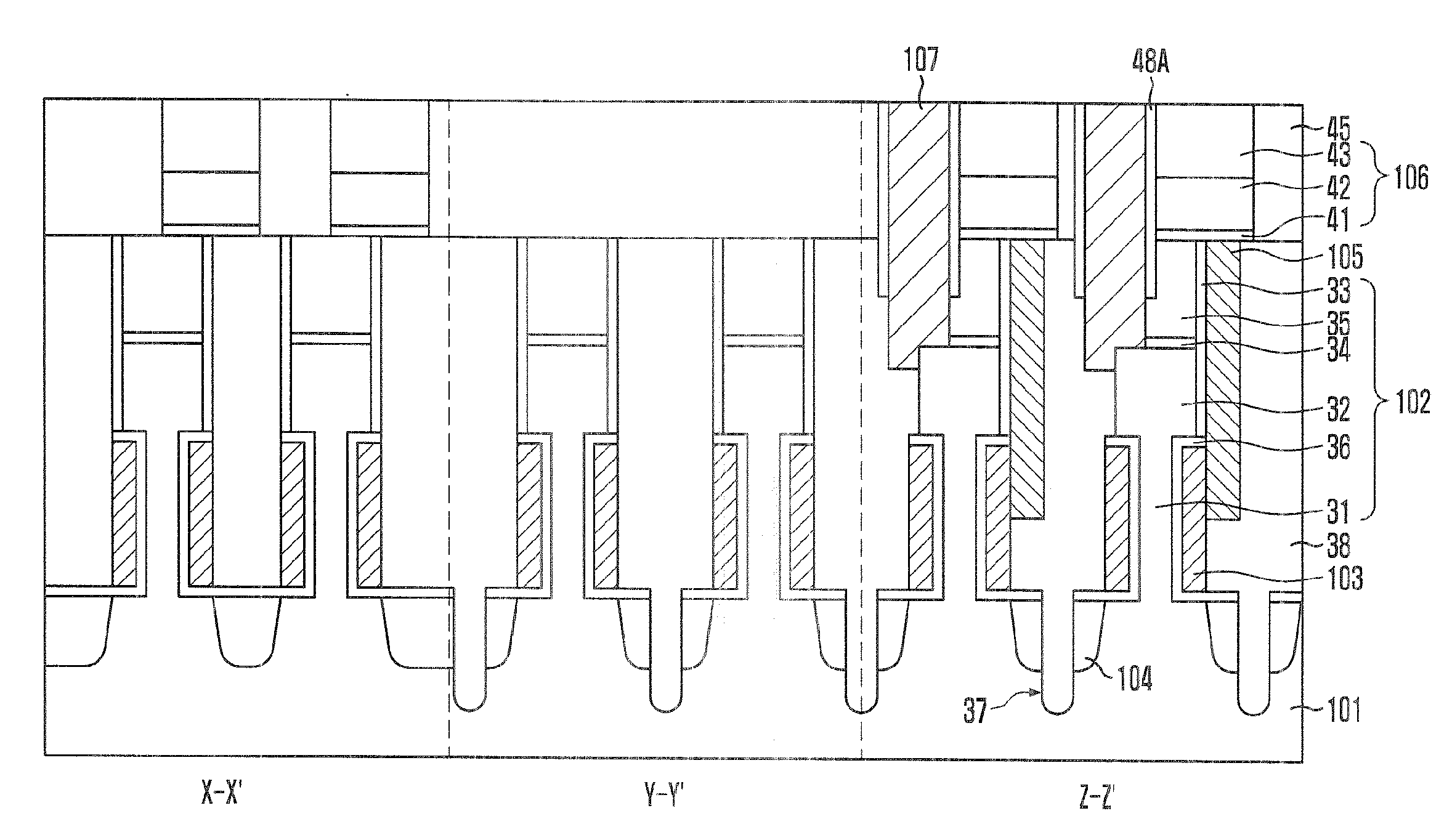
[0030]In FIGS. 2A and 2B, the semiconductor device includes a plurality of pillar structures 102 disposed on a substrate 101, a gate electrode 103 surrounding a lower outer wall of the pillar structure 102, a first interlayer dielectric (ILD) layer 38 insulating the neighboring pillar structures 102 from each other, a gate contact 105 penetrating the first ILD layer 38 to be connected to a sidewall of the gate electrode 103, and a word li...


PUM


Abstract

A semiconductor device having a substrate; a plurality of pillar structures, wherein each pillar structure includes an active pillar disposed over the substrate; a gate electrode surrounding an outer wall of the active pillar; an interlayer dielectric (ILD) layer insulating adjacent pillar structures; a gate contact penetrating the ILD layer and configured to connect to a sidewall of the gate electrode; and a word line connected to the gate contact.

Description

CROSS-REFERENCE TO RELATED APPLICATIONS[0001]The present application claims priority of Korean patent application number 10-2008-0026421, filed on Mar. 21, 2008, which is incorporated by reference herein in its entirety.BACKGROUND[0002]There are increasing demands for 40 nm memory devices with a linewidth of 40 nm and less in order to increase the degree of integration. However, it is very difficult to realize a downscaled memory device having a linewidth of 40 nm or less using a typical planar or recessed gate transistor having 8F2 or 6F2 cell architecture, (the capital letter ‘F’ represents a minimum feature size). Therefore, DRAM devices with 4F2 cell architecture are increasingly demanded because this architecture can improve the degree of integration by 1.5 to 2 times higher without scale-down.[0003]In a vertical channel transistor, a surround type gate electrode is formed to surround an active pillar that extends vertically on a semiconductor substrate, and source and drain re...

Claims


Application Information

Patent Timeline
Patent Type & Authority Applications(United States)
IPC IPC(8): H01L29/78H01L21/28H10B12/00
CPCH01L27/10876H01L29/7827H01L27/108H01L27/10891H10B12/053H10B12/488H10B12/395H10B12/0383H10B12/00
Inventor SUNG, MIN-GYUKIM, YONG-SOOLIM, KWAN-YONG
Owner SK HYNIX INC
Learn More