Liquid Crystal Display Device

a liquid crystal display and display device technology, applied in non-linear optics, instruments, optics, etc., can solve problems such as leakage current, achieve the effects of suppressing the increase of manufacturing cost, reducing the manufacturing cost of tft with channel stopper, and favorable current characteristi

Inactive Publication Date: 2009-09-10
PANASONIC LIQUID CRYSTAL DISPLAY CO LTD +1
View PDF1 Cites 40 Cited by
  • Summary
  • Abstract
  • Description
  • Claims
  • Application Information

AI Technical Summary

Benefits of technology

[0015]FIG. 16 is a cross-sectional view of a TFT which overcomes such a drawback. In FIG. 16, a poly-Si layer 107 and an a-Si layer 108 are formed on a gate electrode 103 with a gate insulation film 104 sandwiched therebetween. The a-Si layer 108 has a film thickness thereof decreased at a portion where a channel etching portion 114 is formed. A passivation film 116 made of SiN is formed so as to cover the channel etching portion 114 and the whole TFT. The constitution shown in FIG. 16 is characterized in that an n+Si layer 109 covers not only an upper surface of the a-Si layer 108 but also side portions of the a-Si layer 108 and side portions of the poly-Si layer 107. Due to such constitution, a depletion layer is formed by forming the n+Si layer 109 between the a-Si layer 108 and the SD electrode 113 as well as between the poly-Si layer 107 and the SD electrode 113 thus preventing the transmission of holes. Accordingly, the TFT having the constitution shown in FIG. 16 can prevent the increase of a quantity of an OFF current.
[0018]To stabilize an operation of the TFT without forming the channel etching layer 114, a channel stopper described later may be formed. However, the formation of the channel stopper and the provision of a surface contact between the poly-Si layer and the SD electrode increase the number of photolithography steps and hence, a manufacturing cost is pushed up.
[0019]It is an object of the present invention to realize the constitution which allows a poly-Si TFT of a bottom gate type to ensure a sufficient ON current while suppressing the increase of a manufacturing cost thereof.
[0031]According to the constitution of the liquid crystal display device of the present invention, it is possible to realize the poly-Si TFT of a bottom gate type while maintaining a favorable ON current characteristic. Accordingly, it is possible to rationally form the drive circuit which includes the TFT in the periphery of the display region.
[0032]Further, according to the present invention, using the same process, the a-Si TFTs can be formed in the display region and the poly-Si TFT can be formed in the drive circuit region and hence, it is possible to realize the liquid crystal display device which incorporates the drive circuit in the substrate while suppressing the increase of a manufacturing cost.
[0033]Still further, according to the present invention, the channel stopper and the poly-Si layer or the a-Si layer can be formed into desired shapes respectively by performing a photolithography process one time and hence, a manufacturing cost of the TFT having the channel stopper can be reduced.

Problems solved by technology

However, this constitution has a drawback that a leak current is generated when the transistor is turned off.

Method used


Image

  • Liquid Crystal Display Device
  • Liquid Crystal Display Device
  • Liquid Crystal Display Device

Examples


embodiment 1

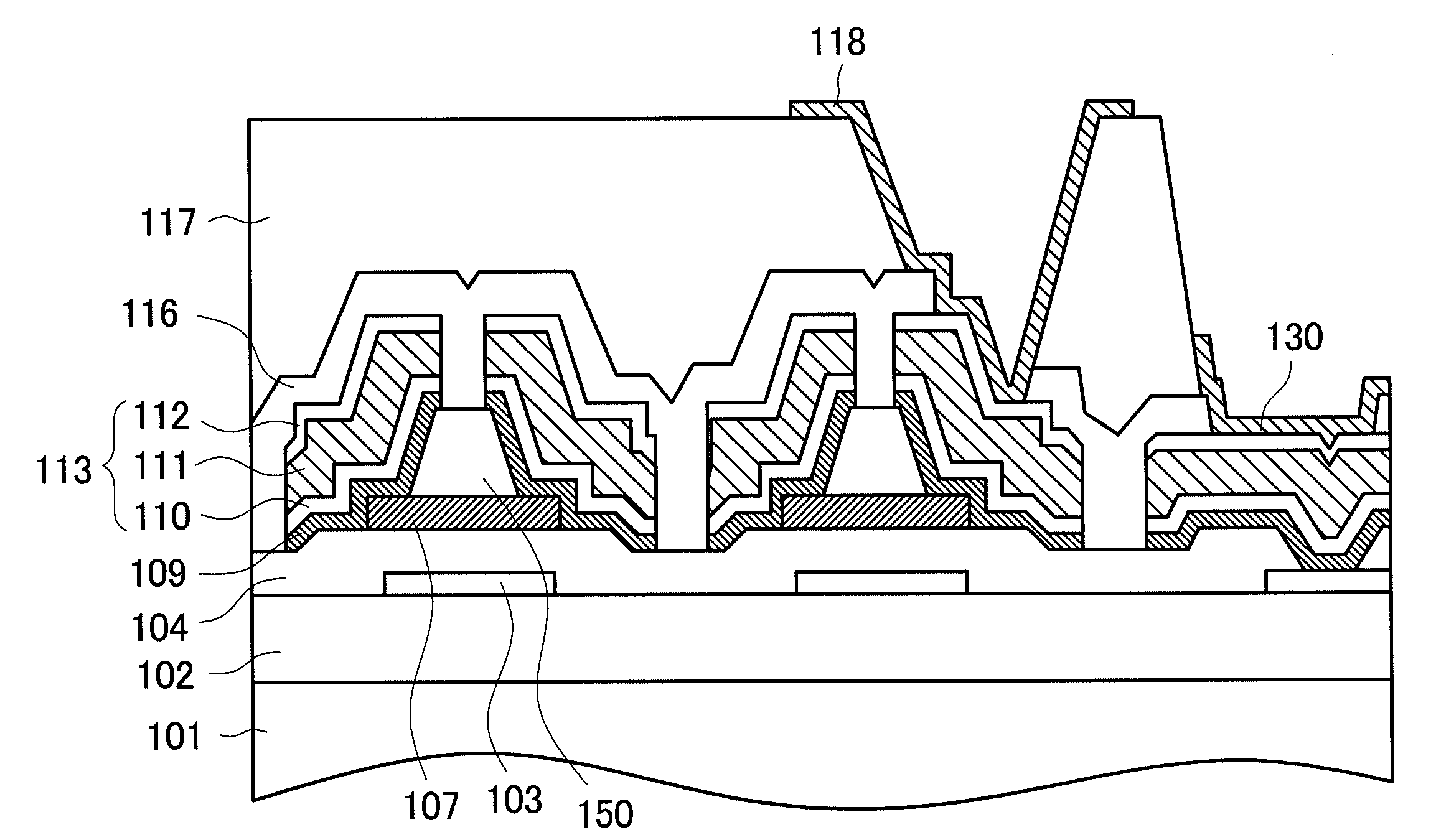
[0051]A liquid crystal display device of this embodiment includes a plurality of pixels each of which is formed in a region surrounded by video signal lines which extend in the longitudinal direction and are arranged parallel to each other in the lateral direction and scanning signal lines which extend in the lateral direction and are arranged parallel to each other in the longitudinal direction, wherein a pixel electrode and a TFT for switching are arranged in each pixel. The pixels each of which includes the pixel electrode and the TFT are arranged in a display region in a matrix array. On the periphery of the display region, a drive circuit which controls the supply of video signals to the respective pixels is arranged. In this embodiment, both of the TFT used in the pixel (pixel-use TFT) and a TFT used in the drive circuit (drive-circuit-use TFT) are formed using a bottom-gate-type poly-Si TFT. Here, the poly-Si TFT is a TFT in which a semiconductor is formed using poly-Si.

[0052...

embodiment 2

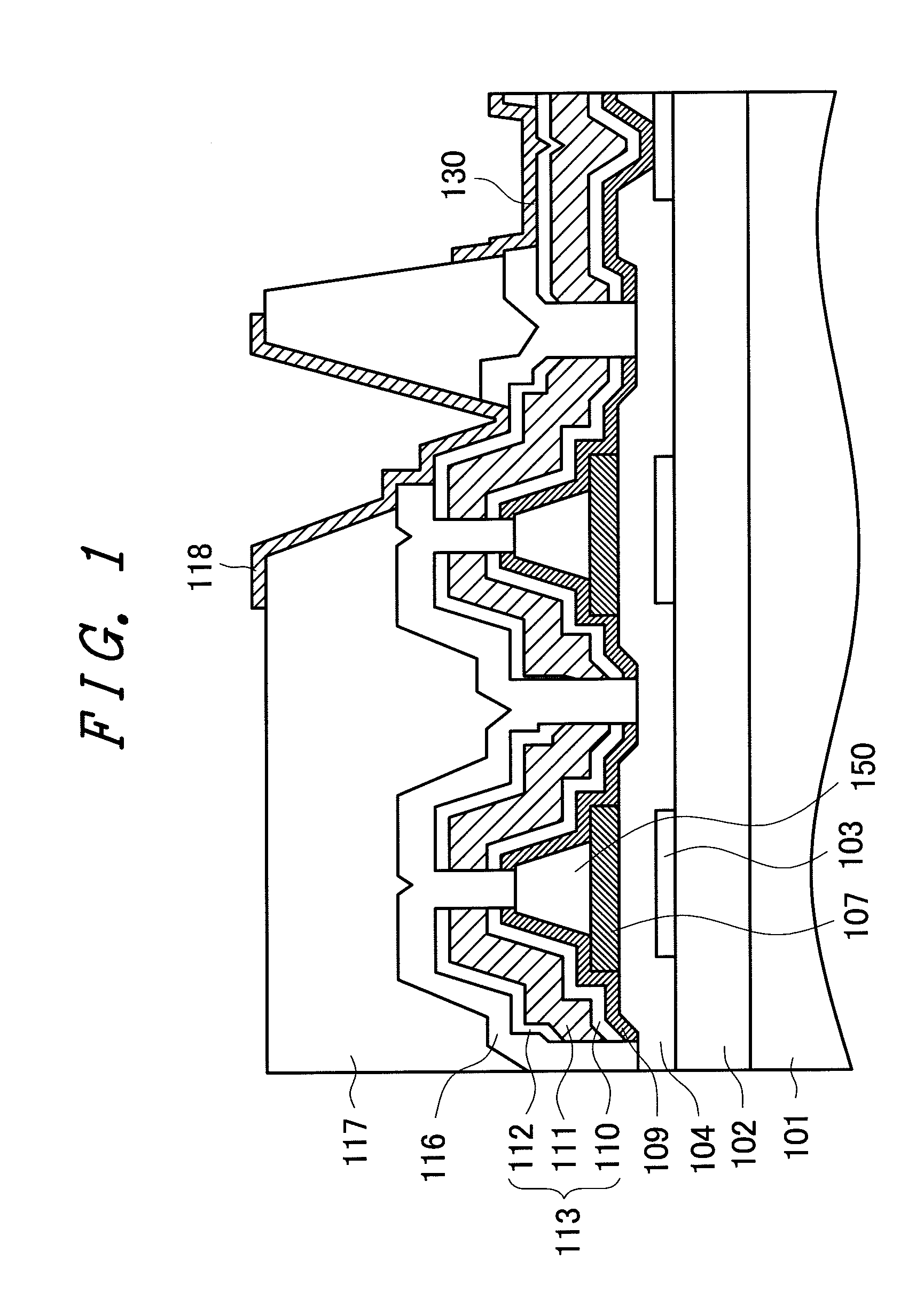
[0072]In this embodiment, the pixel-use TFT is an a-Si TFT of a bottom gate type, and the drive-circuit-use TFT is a poly-Si TFT of a bottom gate type. Here, the a-Si TFT is a TFT in which a semiconductor layer is formed using a-Si, and the poly-Si TFT is a TFT in which a semiconductor layer is formed using poly-Si. The poly-Si TFT which exhibits large mobility thus operating at a high speed is advantageous in the drive circuit part, and the a-Si TFT which can easily decrease a leak current is advantageous in the pixel part.

[0073]FIG. 10 is a schematic cross-sectional view showing the constitution of a portion of the liquid crystal display device of the embodiment 2 according to the present invention. In FIG. 10, the left-side TFT is a drive-circuit-use TFT, and a semiconductor layer of the TFT is made of poly-Si. Since the drive-circuit-use TFT requires a high-speed operation, the TFT in which the semiconductor layer is formed using poly-Si is used. The right-side TFT is a pixel-us...


PUM


Abstract

In bottom-gate-type thin film transistors used in a liquid crystal display device, a channel stopper layer is formed on a poly-Si layer thus stabilizing a characteristic of the thin film transistor. The channel stopper layer is formed into a desired shape by wet etching, and the poly-Si layer is formed into a desired shape by dry etching. By applying side etching to the channel stopper layer, a peripheral portion of the poly-Si layer is exposed from the channel stopper layer, and this region is brought into contact with an n+Si layer. Due to such constitution, ON resistance of the thin film transistor can be decreased thus increasing an ON current which flows in the thin film transistor.

Description

[0001]The present application claims priority from Japanese applications JP2008-056718 filed on Mar. 6, 2008, the content of which is hereby incorporated by reference into this application.BACKGROUND OF THE INVENTION[0002]1. Field of the Invention[0003]The present invention relates to a display device, and more particularly to a liquid crystal display device which forms pixels using thin film transistors (TFTs) as switching elements in a display region and arranges a drive circuit formed of a TFT whose channel portion is made of poly-Si on the periphery of the display region.[0004]2. Description of the Related Art[0005]In a liquid crystal display device, a TFT substrate on which pixel electrodes and thin film transistors (TFTs) and the like are formed in a matrix array, and a color filter substrate on which color filters and the like are formed at positions corresponding to the pixel electrodes are arranged to face each other in an opposed manner, and liquid crystal is sandwiched be...

Claims


Application Information

Patent Timeline
IPC IPC(8): G02F1/136H01L33/00G02F1/1345G02F1/1368H01L21/336H01L29/786
CPCG02F1/1303G02F1/1368G02F2202/103H01L29/78609H01L27/1214H01L29/66765G02F2202/104H01L27/1288
Inventor KAITOH, TAKUOSONODA, DAISUKENITTA, HIDEKAZU
Owner PANASONIC LIQUID CRYSTAL DISPLAY CO LTD
Why Eureka
Try Eureka