Touch panel and touch-panel device
a touch panel and display device technology, applied in the field of touch panels, can solve the problems of reducing the total thickness affecting the light performance of the display device, and reducing the light transparency, so as to improve the total sensing performance of the touch panel, reduce the total fabrication cost and volume of the flat display device, and minimize electronic products
- Summary
- Abstract
- Description
- Claims
- Application Information
AI Technical Summary
Benefits of technology
Problems solved by technology
Method used
Image
Examples
first embodiment
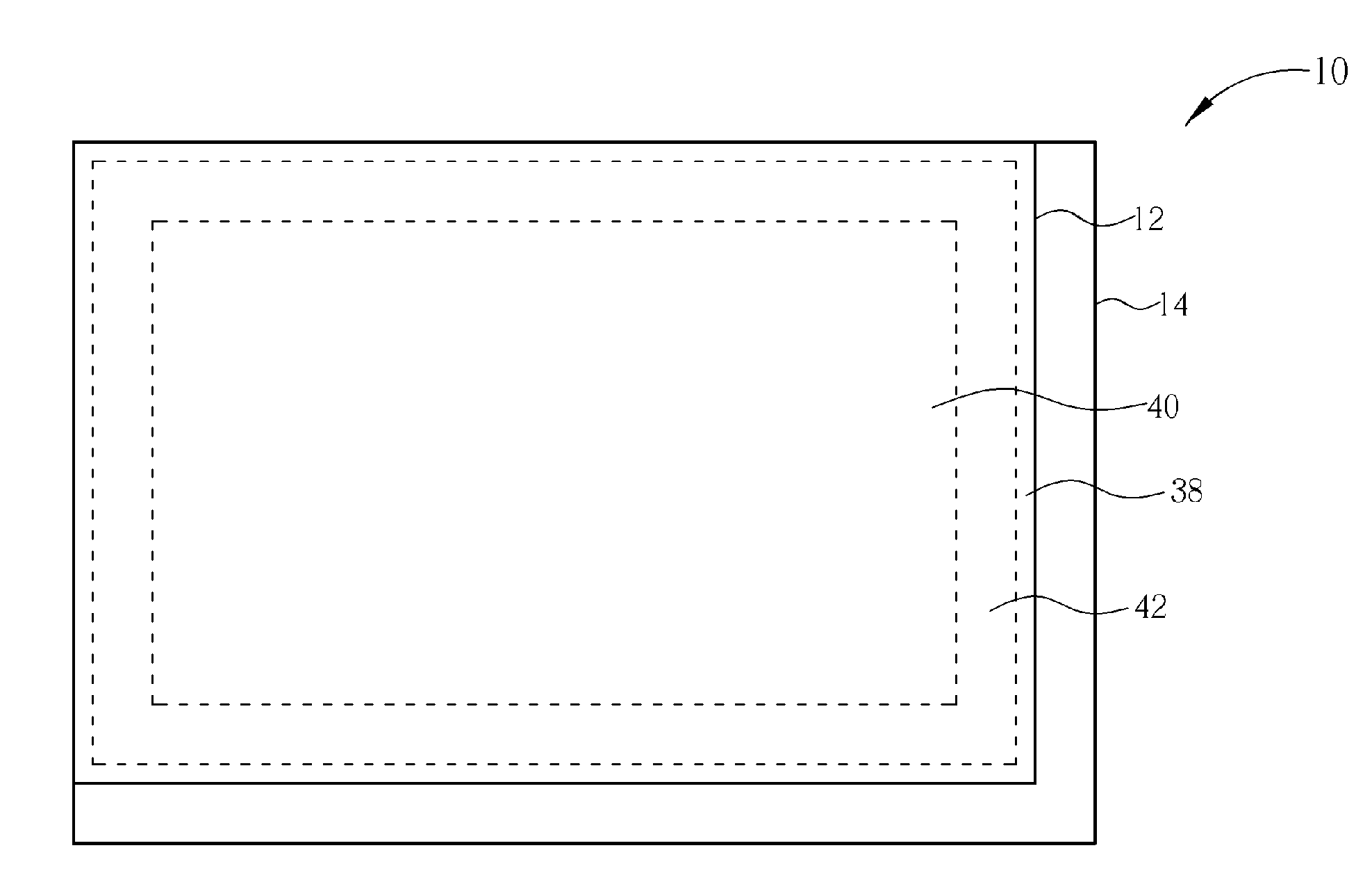
[0019]FIG. 1 to FIG. 3 are schematic diagrams of an in-cell touch panel (integrated touch panel) 10 according to the present invention, wherein FIG. 1 is a top view of the in-cell touch panel 10 of the present invention, FIG. 2 shows the arrangement of partial elements of the in-cell touch panel 10 shown in FIG. 1, and FIG. 3 is an equivalent circuit diagram of the in-cell touch panel 10. The in-cell touch panel 10 of the present invention is a flat panel having touch control and display functions at the same time. In this embodiment, a multi-touch control device is integrated in an LCD panel. The in-cell touch panel 10 comprises a first substrate 12, a second substrate 14, and a liquid crystal layer 48 positioned between the first substrate 12 and the second substrate 14. The first substrate 12 and the second substrate 14 are preferably formed with glass or quartz materials, and are fixed with a sealant located between the both substrates. Wherein, the first substrate 12 generally ...
second embodiment
[0025]Referring to FIG. 5 and FIG. 6, FIG. 5 is a schematic diagram of top view of an in-cell touch panel according to the present invention, and FIG. 6 is a schematic diagram of sectional view of partial elements of the in-cell touch panel shown in FIG. 5. The present invention in-cell touch panel 100 comprises a first substrate 102 and a second substrate 104 parallel to each other, wherein both of them are fixed by a sealant 128 and disposed opposite. The sealant 128 is disposed inside the sealant region 106. In order to improve the disadvantage of the conventional touch panel that more active force is required to be applied onto the portion of the conventional touch panel closer to the sealant region for producing sensing signals, the present invention in-cell touch panel 100 comprises pluralities of sensing zones from the central portion to the periphery portion of the display region. For example, the in-cell touch panel 100 comprises a first sensing zone 108 disposed in the cen...
PUM
 Abstract
Description
Claims
Application Information
 - R&D
- Intellectual Property
- Life Sciences
- Materials
- Tech Scout
- Unparalleled Data Quality
- Higher Quality Content
- 60% Fewer Hallucinations
Browse by: Latest US Patents, China's latest patents, Technical Efficacy Thesaurus, Application Domain, Technology Topic, Popular Technical Reports.
© 2025 PatSnap. All rights reserved.Legal|Privacy policy|Modern Slavery Act Transparency Statement|Sitemap|About US| Contact US: help@patsnap.com


