NAND flash memory array with cut-off gate line and methods for operating and fabricating the same
a technology gate line, which is applied in the field of nand flash memory array, can solve problems such as the limitation of improving integrity degree, and achieve the effect of reducing the area of separating conventional control gates and minimizing the effect of storage condition
- Summary
- Abstract
- Description
- Claims
- Application Information
AI Technical Summary
Benefits of technology
Problems solved by technology
Method used
Image

Examples
first embodiment
[First Embodiment of an Array Operating Method]
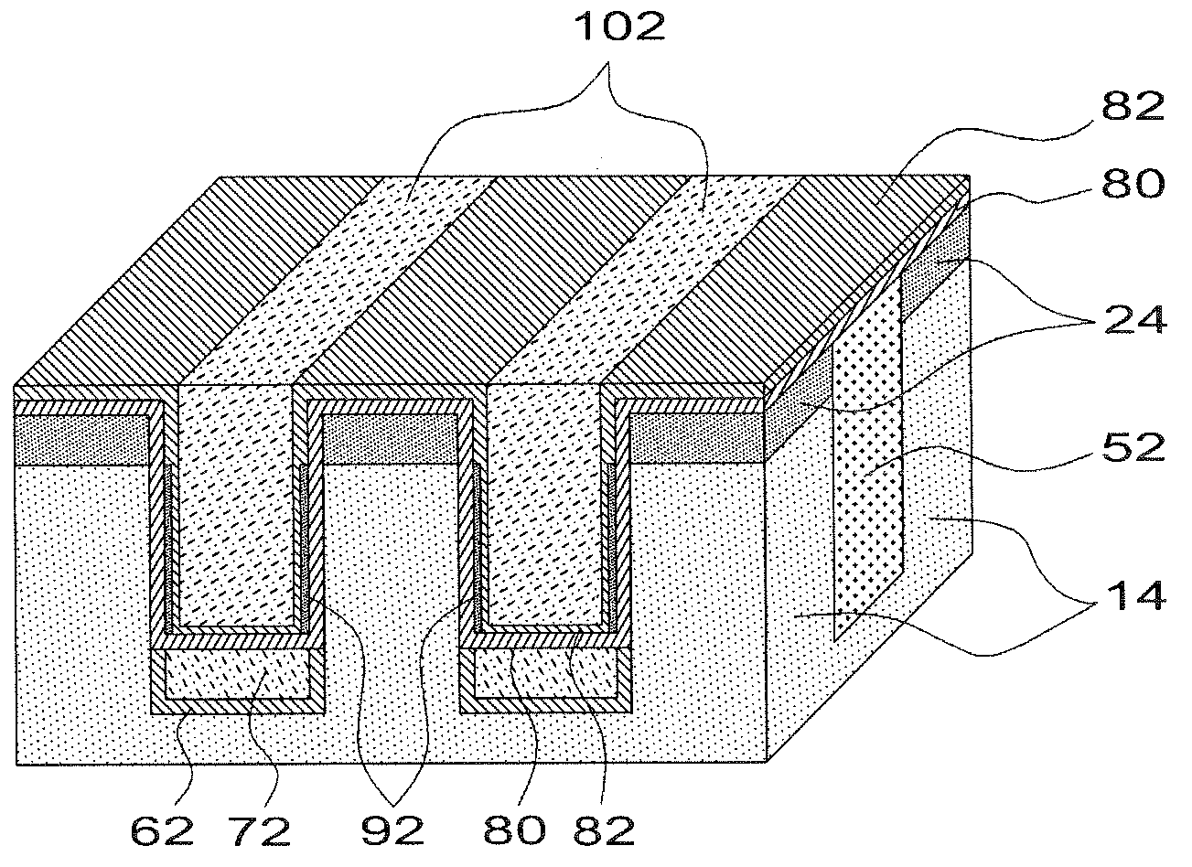
[0042]First, a method for programming a NAND flash memory array of the second embodiment of an array structure, is characterized by programming one of two memory cells first which formed at the site where one of the bit lines and one of the word lines cross each other by applying an appropriate bias voltage to the common source line, the power supply line, the each first selective line, the each second selective line, the each bit line, the each word line, the each cut-off gate line and the silicon substrate, respectively, and then programming the other cell by changing the bias voltage condition.
[0043]More specifically, as shown in FIG. 4b, in order to program one memory cell toward the common source line (not shown in Fig.) in the two memory cells operated by the word line 102b by injecting electrons into the charge storage layer 92c, the common source line is grounded, a voltage Vcc is applied to the power supply line, respectively, ...
second embodiment
[Second Embodiment of an Array Operating Method]
[0051]Next, the first embodiment of operating method for a NAND flash memory array of the second embodiment of an array structure, is further characterized by erasing memory cells of a block to be connected to a word line passing a specific cell at a time by grounding the word line passing the specific cell to erase information and the cut-off gate line passing under the word line, floating the other lines, and applying a voltage, which is high enough to pull out electrons from a charge storage layer of the specific cell or to inject holes from a channel region of the specific cell to the charge storage layer of the specific cell, to the silicon substrate.
[0052]Because the method for erasing can be embodied satisfactorily by the above explanation, its detailed explanation is omitted.
third embodiment
[Third Embodiment of an Array Operating Method]
[0053]In the meantime, the first embodiment of operating method for a NAND flash memory array of the second embodiment of an array structure, is further characterized by reading information of a specific cell by applying a proper bias voltage respectively to the common source line, the power supply line, the each first selective line, the each second selective line, the each bit line, the each word line, the each cut-off gate line and the silicon substrate to turn on only the first selective transistor and the second selective transistor connected to both ends of a bit line passing the specific cell desired to be read information, and measuring current which flows from the power supply line to the common source line on a specific standard voltage applied to a word line passing the specific cell.
[0054]Here, it is more preferable that reading information of the specific cell is by changing a bias voltage condition of the common source lin...
PUM
 Abstract
Description
Claims
Application Information
 - R&D
- Intellectual Property
- Life Sciences
- Materials
- Tech Scout
- Unparalleled Data Quality
- Higher Quality Content
- 60% Fewer Hallucinations
Browse by: Latest US Patents, China's latest patents, Technical Efficacy Thesaurus, Application Domain, Technology Topic, Popular Technical Reports.
© 2025 PatSnap. All rights reserved.Legal|Privacy policy|Modern Slavery Act Transparency Statement|Sitemap|About US| Contact US: help@patsnap.com