
Variable-impedance gated decoupling cell

Active Publication Date: 2009-06-18
SYNOPSYS INC
View PDF5 Cites 14 Cited by
  • Summary
  • Abstract
  • Description
  • Claims
  • Application Information

AI Technical Summary

Benefits of technology

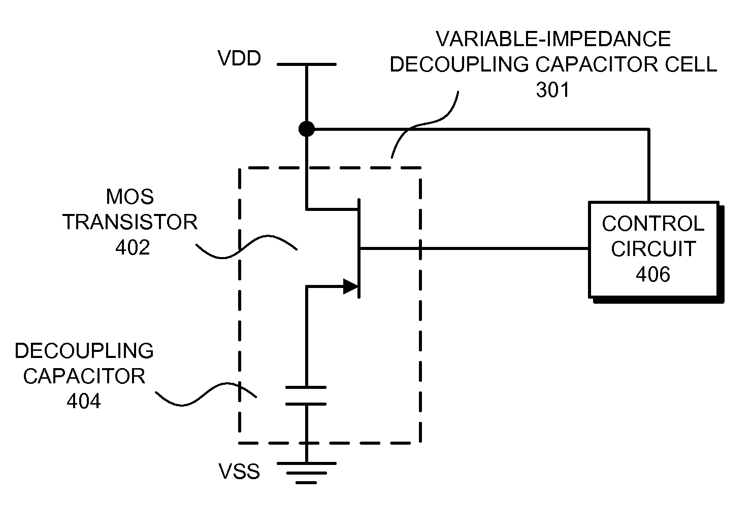
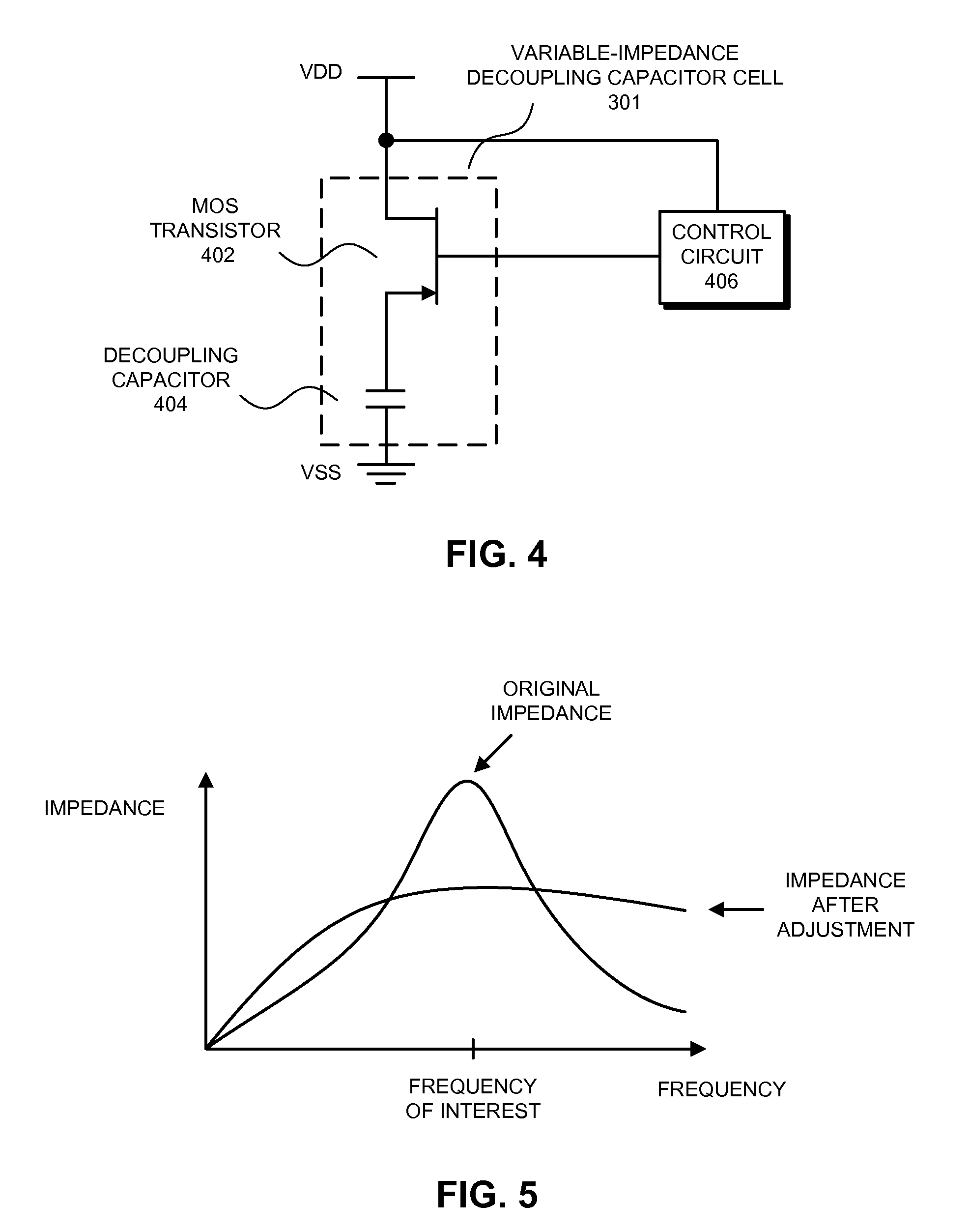
[0015]In some embodiments of the present invention, the control circuit is configured to increase the impedance of the MOS transistor to decrease the noise in the frequency range near ωinterest or decrease the impedance of the MOS transistor to decrease the switching noise at other frequencies.
[0019]Embodiments of the present invention provide a system that controls noise in a power system that includes a power rail and a ground rail, wherein a first lead of a decoupling capacitor is coupled to the ground rail, a MOS transistor is coupled in series with the decoupling capacitor, with a source of the MOS transistor coupled to the power rail and a drain of the MOS transistor coupled to a second lead on the decoupling capacitor, and an inductive packaging connection is coupled to the power rail, and wherein the MOS transistor and the decoupling capacitor are configured to be in parallel with the inductive packaging connection, thereby forming a resonant circuit. The system starts by determining if there is noise in a Vdd signal on the power rail. Then, based on the noise in the Vdd signal, the system adjusts a voltage applied to the gate of the MOS transistor, thereby changing an impedance of the MOS transistor to reduce the noise in a frequency range near a ωinterest of the resonant circuit without causing an unnecessary increase in switching noise at other frequencies.
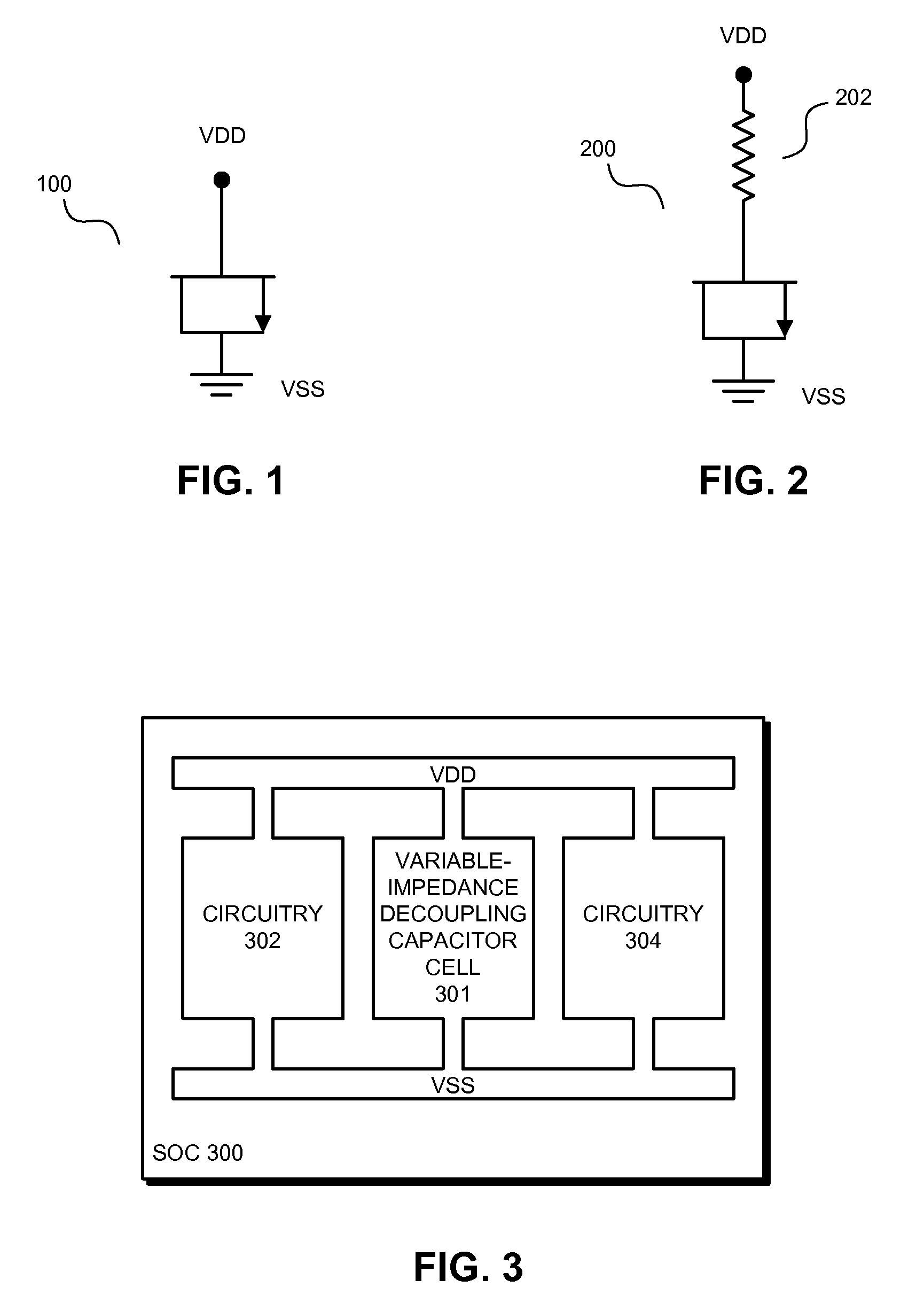
[0020]Embodiments of the present invention provide a semiconductor chip for controlling noise in a power system that includes a power rail and a ground rail. The SOC comprises: (1) a set of circuitry coupled between the power rail and the ground rail, wherein the power rail and the ground rail provide electrical power and ground for the set of circuitry; (2) a decoupling capacitor having a first lead which is coupled to the ground rail; (3) a MOS transistor coupled in series with the decoupling capacitor, wherein a source of the MOS transistor is coupled to the power rail and a drain of the MOS transistor is coupled to a second lead on the decoupling capacitor; and (4) an inductive packaging connection coupled to the power rail. The MOS transistor and the decoupling capacitor are configured to be in parallel with the inductive packaging connection, thereby forming a resonant circuit. In addition, the system includes a control circuit within an input coupled to the power rail and an output coupled to a gate of the MOS transistor. During operation, the control circuit monitors a noise in the Vdd signal. The control circuit is configured to adjust a voltage applied to the gate of the MOS transistor based on the noise in the Vdd signal, thereby changing an impedance of the MOS transistor to reduce the noise in a frequency range near a ωinterest of the resonant circuit without causing an unnecessary increase in switching noise at other frequencies.

Problems solved by technology

Unfortunately, the parallel combination of the inductive packaging connection to Vdd and on-chip decoupling capacitors creates a resonant LC circuit whose impedance can be high in a range of frequencies near a resonance frequency (ωres).
Unfortunately, while eliminating noise near ωres, this technique can reduce the efficiency of the decoupling capacitors for controlling noise in the Vdd signal in other frequency ranges.
Unfortunately, the MOS transistors in these systems are either “ON” or “OFF,” and in circumstances where the MOS transistors are ON, the system can still experience excessive noise near ωres.

Method used


Image

  • Variable-impedance gated decoupling cell
  • Variable-impedance gated decoupling cell
  • Variable-impedance gated decoupling cell

Examples


Embodiment Construction

[0029]The following description is presented to enable any person skilled in the art to make and use the invention, and is provided in the context of a particular application and its requirements. Various modifications to the disclosed embodiments will be readily apparent to those skilled in the art, and the general principles defined herein may be applied to other embodiments and applications without departing from the spirit and scope of the present invention. Thus, the present invention is not limited to the embodiments shown, but is to be accorded the widest scope consistent with the claims.

Overview

[0030]Embodiments of the present invention provide a variable-impedance decoupling capacitor cell that can be used to reduce power system noise in many different types of semiconductor chips, such as a “system on a chip” (SOC), a processor, an application-specific integrated circuit (ASIC), or another type of semiconductor chip that includes integrated circuits.

[0031]The variable-impe...


PUM


Abstract

Embodiments of the present invention provide a system that controls noise in a power system that includes a power rail and a ground rail. The system includes a MOS transistor coupled in series with a decoupling capacitor between the power rail and the ground rail and an inductive packaging connection coupled to the power rail in parallel with the MOS transistor and the decoupling capacitor. The combination of MOS transistor, decoupling capacitor, and inductive packaging connection form a resonant circuit. During operation, the system determines if there is noise in a Vdd signal on the power rail. Based on the noise present in the Vdd signal, the system adjusts the impedance of the MOS transistor to reduce the noise in a frequency range near a frequency of interest (ωinterest) of the resonant circuit without causing an unnecessary increase in switching noise at other frequencies.

Description

BACKGROUND[0001]1. Field of the Invention[0002]Embodiments of the present invention relate to circuits. More specifically, embodiments of the present invention relate to the design of a variable-impedance gated decoupling cell.[0003]2. Related Art[0004]Recent developments in integrated circuit technologies have enabled designers to create complex integrated circuits on semiconductor chips which include both digital and analog circuitry. A “system-on-a-chip” (SOC) is one such integrated circuit, which includes different types of circuits that enable the SOC to perform a wide variety of functions. For example, SOCs can include controllers, processors, graphics and audio processors, transceivers, networking devices, communication circuits, memories, and other types of circuits. These functional capabilities enable SOCs to be used in devices such as cell phones, personal digital assistants, embedded systems, portable computers, media players, desktop computers, household electronics and...

Claims


Application Information

Patent Timeline
IPC IPC(8): H03K5/08
CPCH01L27/0811H01L27/0629
Inventor TOFFOLON, DINO A.DIETRICH, CHRIS
Owner SYNOPSYS INC
Learn More