Display device and method for production thereof
- Summary
- Abstract
- Description
- Claims
- Application Information
AI Technical Summary
Benefits of technology
Problems solved by technology
Method used
Image
Examples
first embodiment
The First Embodiment
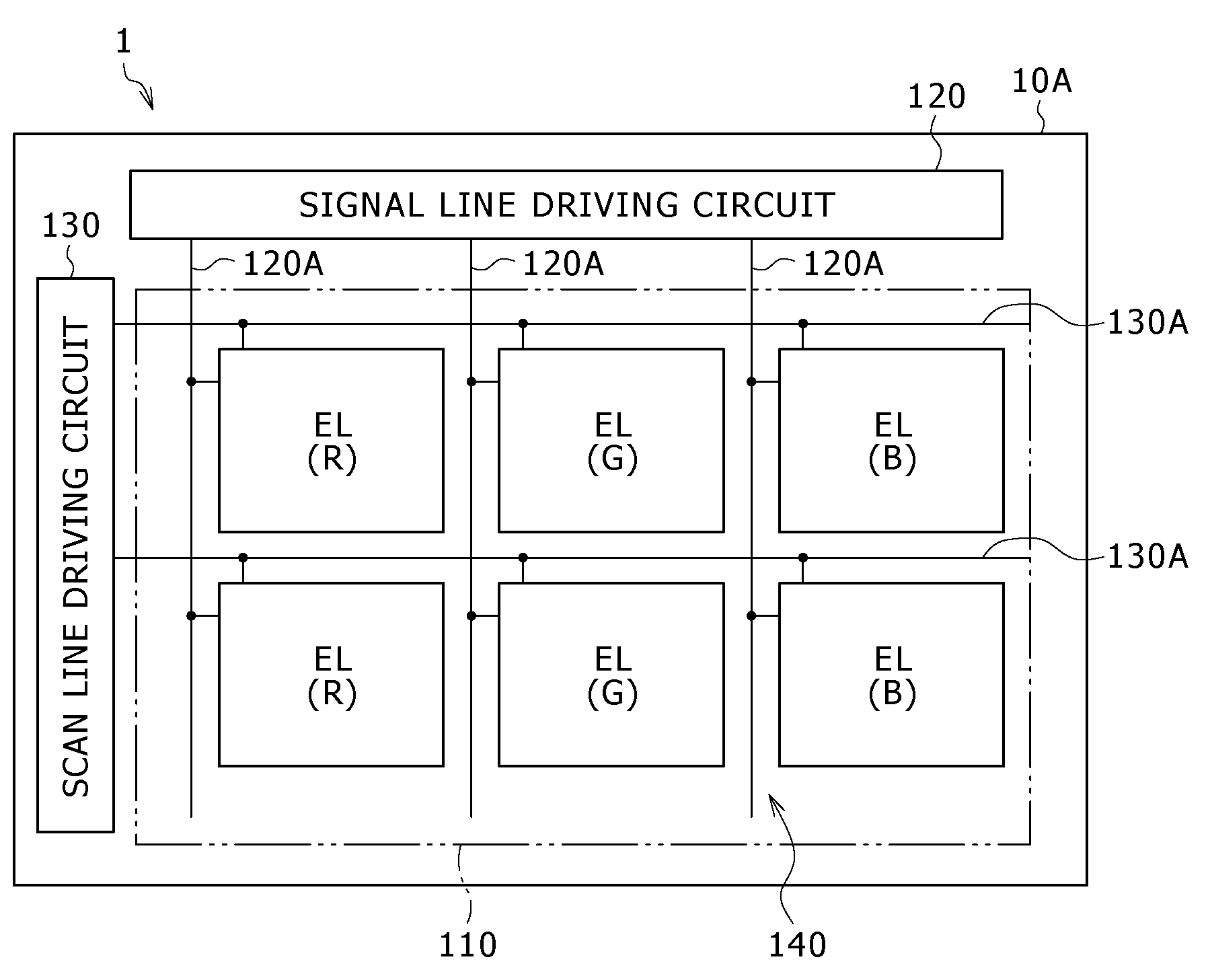
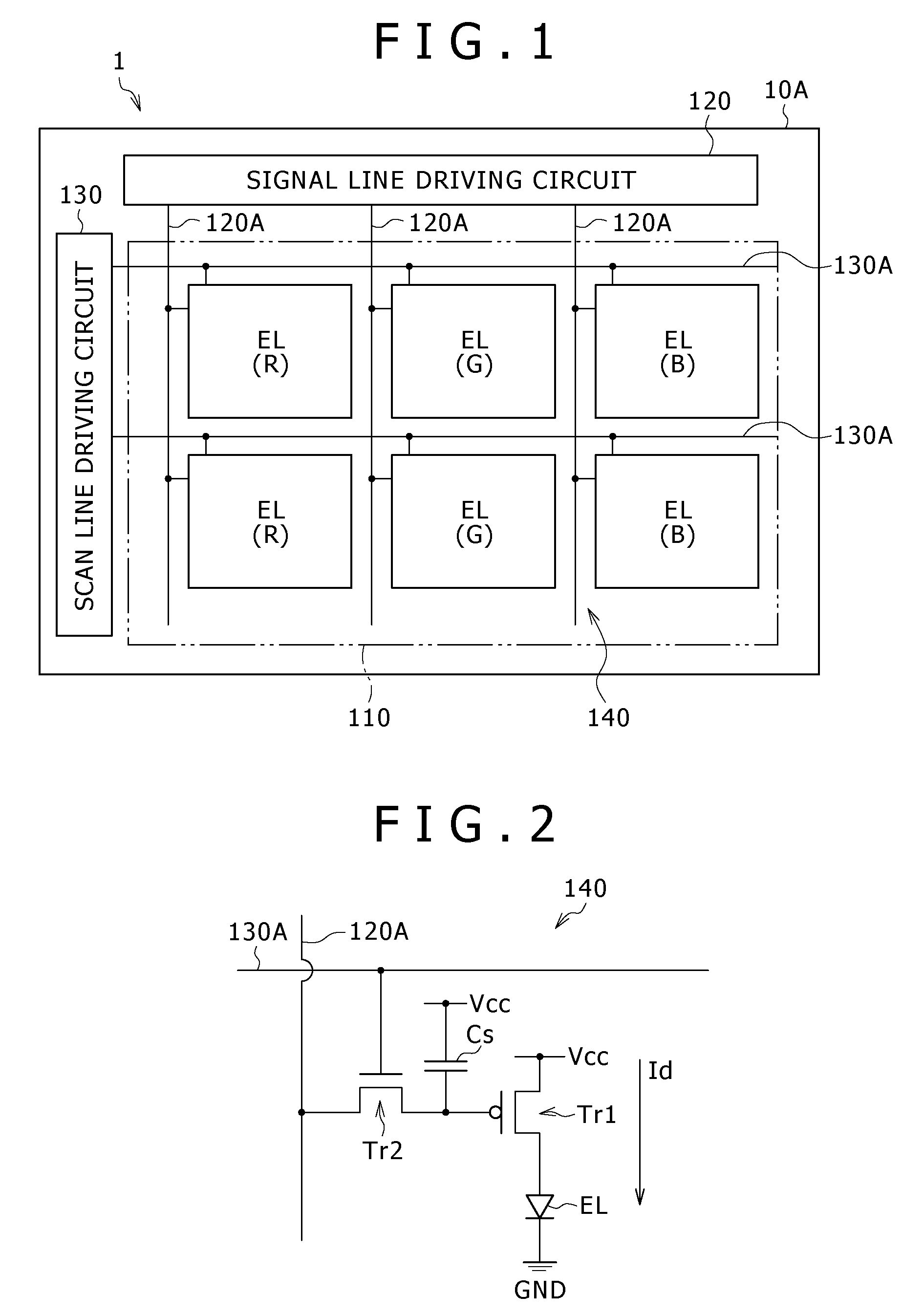
[0049]FIG. 1 is a diagram showing the structure of the display device (organic EL display device) pertaining to the first embodiment of the present invention. The organic EL display device 1 is one which is used as an organic color display device of very thin type. It is composed of a transparent substrate 10A and a plurality of organic EL elements (EL) arranged thereon in a matrix pattern so as to form the display region 110. It also has a signal driving circuit 120 and a scan line driving circuit 130 (both for image display), which are formed along the sides of the display region 110.
[0050]The display region 110 has the pixel driving circuit 140 formed therein. FIG. 2 is a diagram showing an example of the pixel driving circuit 140. The pixel driving circuit 140 is a driving circuit of active type, which is formed under the first electrode 18A (mentioned later) and is composed of a driving transistor Tr1, a writing transistor Tr2, a capacitor Cs (placed between...
second embodiment
The Second Embodiment
[0098]The following deals with the display device pertaining to the second embodiment of the present invention. The constituents common to the first and second embodiments are given the same symbols and their explanation is not repeated.
[0099]FIG. 11 is a sectional view showing the structure of the contact part 25B of the display device (organic EL display device) pertaining to this embodiment. The contact part 25B has on the transparent substrate 11A the low-resistance wiring layer 26 as the lowermost layer which is identical with the source signal line or gate wiring connected to the thin film transistor Tr. The low-resistance wiring layer 26 is 500 nm thick and has the layer identical with the gate electrode 11, the gate insulating layer 12, the silicon film 13A, the stopper insulating film 14, and the n+-amorphous silicon film 13B which are sequentially formed thereon upward. The low-resistance wiring layer 26 prevents the gate wiring, the source signal line...
third embodiment
The Third Embodiment
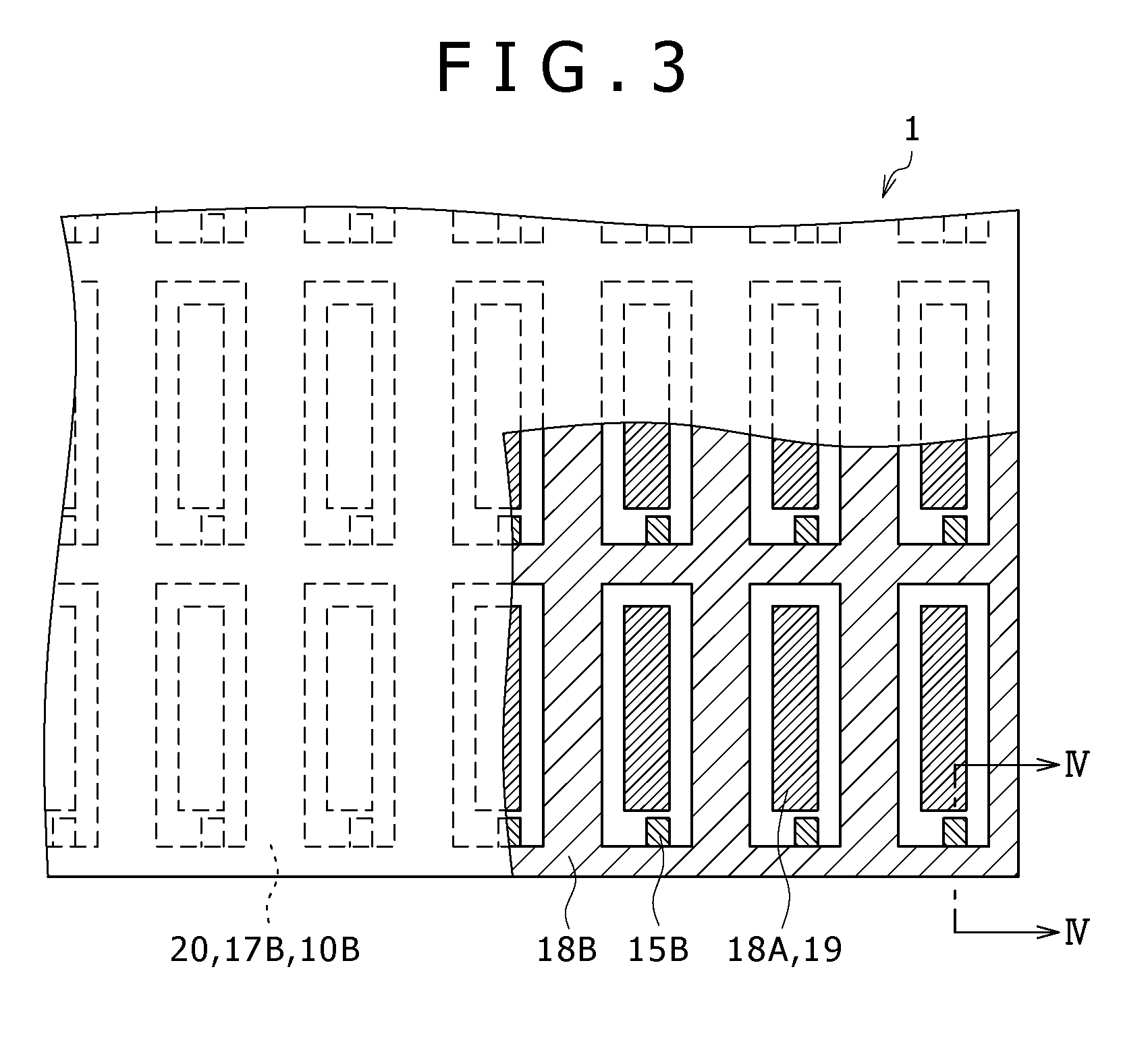
[0108]FIG. 14 is a diagram showing the plane structure of the display region 110 of the organic EL display device 1 according to the third embodiment of the present invention. FIG. 15 is a sectional view taken along the line XV-XV in FIG. 14. This organic EL display device 1 is identical in structure with the one according to the first embodiment mentioned above, except that the auxiliary wiring 15C has the same layered structure as the contact part 15B and is formed integrally with the contact part 15B. Thus, the corresponding constituents are given the same reference characters.
[0109]This embodiment is identical with the first embodiment in that the same structure is adopted for the transparent substrates 10A and 10B, the thin film transistor Tr, the wiring layer 15A, the contact part 15B, the protective insulating film 16, the planarized insulating film 17A, the electrode insulating film 21, the sealing resin 17B, and the organic EL element (EL).
[0110]The auxi...
PUM
 Abstract
Description
Claims
Application Information
 - R&D
- Intellectual Property
- Life Sciences
- Materials
- Tech Scout
- Unparalleled Data Quality
- Higher Quality Content
- 60% Fewer Hallucinations
Browse by: Latest US Patents, China's latest patents, Technical Efficacy Thesaurus, Application Domain, Technology Topic, Popular Technical Reports.
© 2025 PatSnap. All rights reserved.Legal|Privacy policy|Modern Slavery Act Transparency Statement|Sitemap|About US| Contact US: help@patsnap.com


