Organic light emitting device

Inactive Publication Date: 2009-05-21
SAMSUNG ELECTRONICS CO LTD
View PDF6 Cites 8 Cited by
  • Summary
  • Abstract
  • Description
  • Claims
  • Application Information

AI Technical Summary

Benefits of technology

[0009]The present invention provides an organic light-emitting device melting a frit evenly to improve adhesion of the upper and lower substrates of the organic light-emitting device.
[0025]According to the present invention, an organic light-emitting device achieves uniform energy distribution of a laser, which is irradiated on a frit, by disposing a metallic layer under the frit. The frit is thus evenly melted and adhesion improves, and the intrusion of moisture, hydrogen and oxygen in air is stopped, so that defects such as changes in electrical and light-emitting characteristics may be prevented.
[0026]Moreover, the frit is melted by a low power laser, so that damage to the device and wirings under the frit may be prevented.

Problems solved by technology

However, the OLED is vulnerable to hydrogen and oxygen since the OLED includes organic material, which may be easily oxidized by moisture in the air since the cathode electrode includes a metallic material, so that the electrical characteristics and the light-emitting characteristics of the OLED may be deteriorated.
Thus, the frit has poor melting distribution and poor adhesion.

Method used


Image

  • Organic light emitting device
  • Organic light emitting device
  • Organic light emitting device

Examples


first embodiment

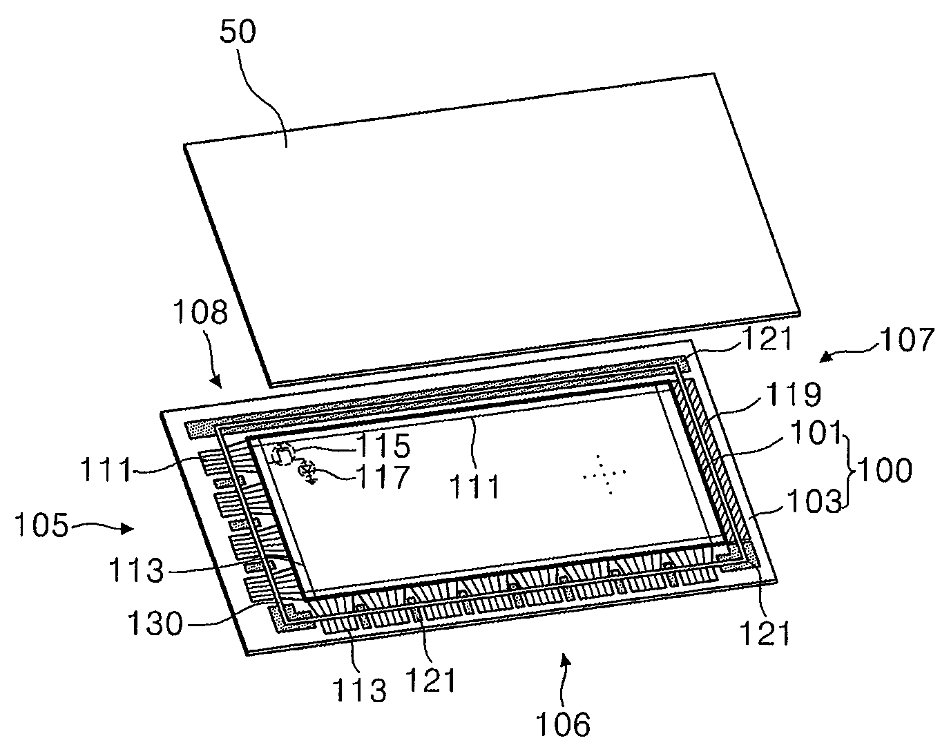
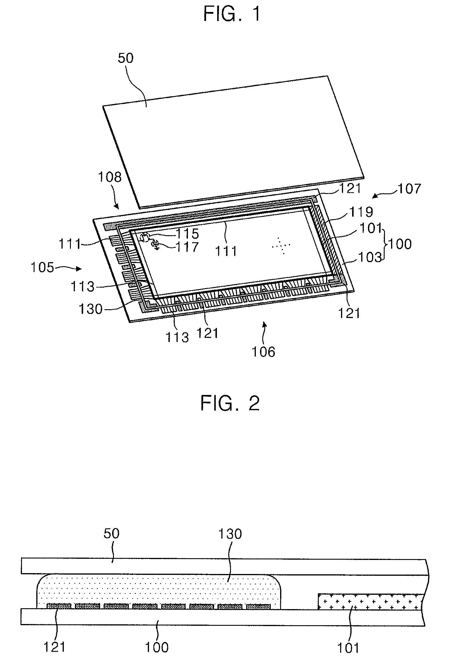
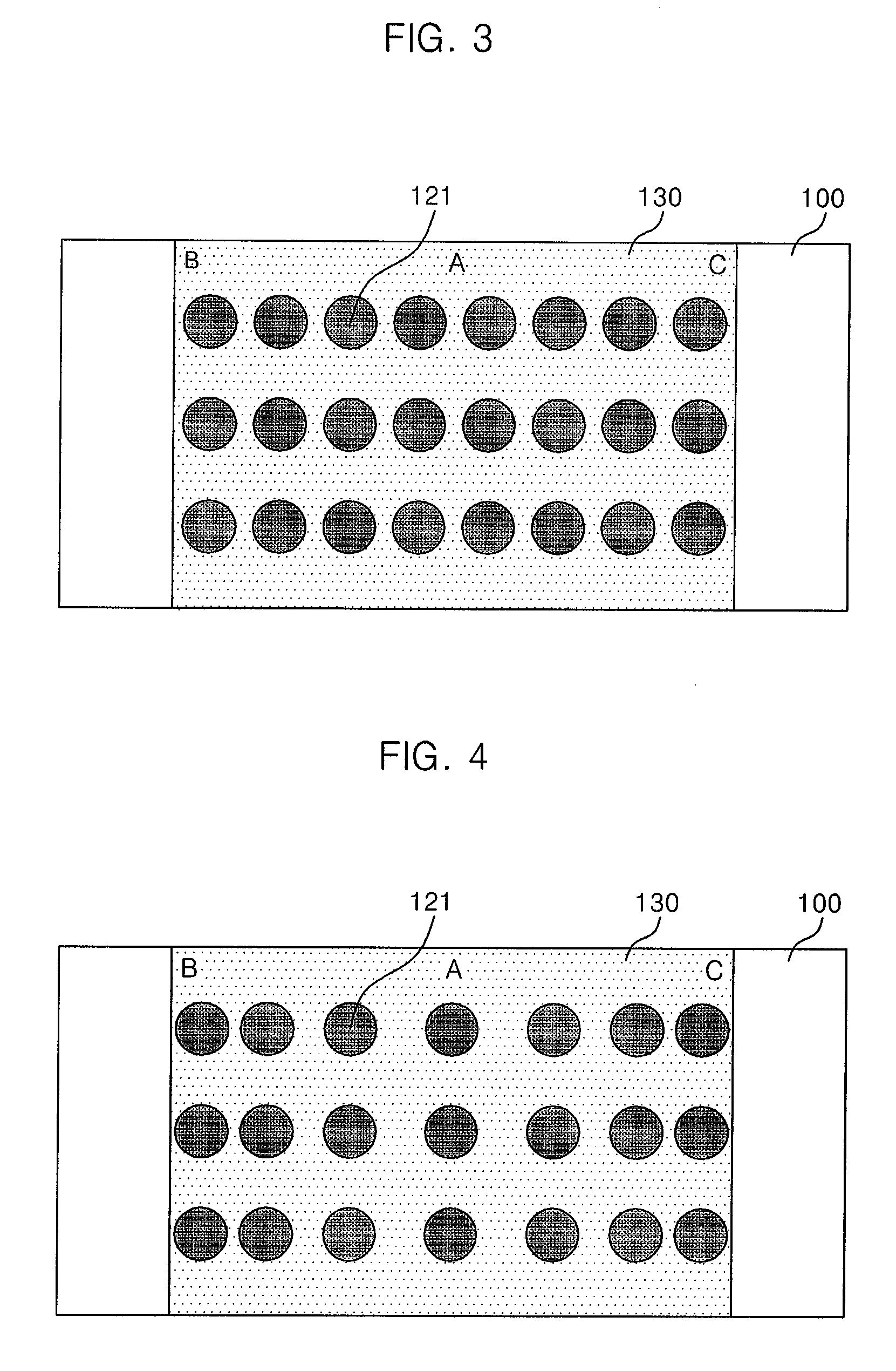
[0059]Referring to FIGS. 2 and 3, an auxiliary metallic layer 121 of an OLED in accordance with the present invention is formed as a dot shape, and is disposed at constant intervals between the edges of frit 130.

[0060]The auxiliary metallic layer 121 is formed on a second substrate 100 to be overlapped by the frit 130. The auxiliary metallic layer 121 may be formed from a plurality of metallic groups, which is formed as one of a circle shape, an elliptical shape and a polygonal shape.

[0061]The auxiliary metallic layer 121 uniformly distributes energies provided to a center A and both sides B and C of the frit 130 when a laser is irradiated on the frit 130.

[0062]A width of a line of the frit 130 is formed to be less than a width of the laser beam which will be used to heat the frit 130. An amount of the laser energy provided to the center A of the frit 130 is greater than the amount of the laser energy provided to sides B and C is low. The frit 130 has difference energy distribution ...

second embodiment

[0067]FIG. 4 is a plan view illustrating a peripheral portion of an OLED in accordance with the present invention.

[0068]Referring to FIG. 4, an auxiliary metallic layer 121 in accordance with the second embodiment of the present invention is formed as a dot shape, and is disposed closer to both sides B and C than to center A of the frit 130. The auxiliary metallic layer 121 may be formed as one of a circle shape, an elliptical shape and a polygonal shape.

[0069]The auxiliary metallic layer 121 uniformly distributes energies provided to the center A and both sides B and C of the frit 130 when a laser is irradiated on the frit 130. The auxiliary metallic layer 121 is disposed denser at both sides B and C of the frit 130 than at the center A of the frit 130, so that the energy, which distributes highly at the center A of the frit 130 and lowly at the sides B and C, automatically becomes uniform by the auxiliary metallic layer 121.

third embodiment

[0070]FIG. 5 is a plan view illustrating a peripheral portion of an OLED in accordance with the present invention.

[0071]Referring to FIG. 5, an auxiliary metallic layer 121 in accordance with the third embodiment of the present invention is formed as a dot shape, and is disposed densely only at both sides B and C of the frit 130. The auxiliary metallic layer 121 may be formed as one of a circle shape, an elliptical shape and a polygonal shape.

[0072]The auxiliary metallic layer 121 highly distributes energy at sides B and C, at which the energy is distributed relatively lowly compared to the center A of the frit 130. Thus, the energy distribution at the center A and both sides B and C of the frit 130 becomes uniform.

[0073]Moreover, the auxiliary metallic layer 121 is not formed at the center A of the frit 130, so that adhesion between the second substrate 100 and the frit 130 is improved.


PUM


Abstract

An organic light-emitting device (“OLED”) improving adhesion of a frit is disclosed. The organic light-emitting device includes a first substrate, an auxiliary metallic layer disposed on a surface of the first substrate, a second substrate, a frit formed in overlapping relationship with the auxiliary metallic layer and interposed between the first and the second substrates to adhere the first and the second substrates together and wherein the auxiliary metallic layer is overlapped by the frit on the first substrate and formed separately from a wiring.

Description

CROSS-REFERENCE TO RELATED APPLICATIONS[0001]This application claims priority under 35 U.S.C. §119 to Korean Patent Application No. 10-2007-0117382, filed on Nov. 16, 2007 in the Korean Intellectual Property Office (KIPO), the contents of which are herein incorporated by reference in their entirety.BACKGROUND OF THE INVENTION[0002]1. Field of the Invention[0003]The present invention relates to an organic light-emitting device. In particular, the present invention relates to an organic light-emitting device having a frit, or a fused or partially fused material.[0004]2. Description of the Related Art[0005]Display devices that display information onto a screen have been improved for high performance by becoming thinner, lighter, and more portable, aiding the development and progression of liquid crystal displays, one of the most important technologies of the modern information age. The Organic light emitting display (“OLED”) has developed as a substitute for the cathode ray tube (“CRT”...

Claims


Application Information

Patent Timeline
IPC IPC(8): H01J1/62
CPCH01L27/3244H05B33/04H01L51/5246H10K59/12H10K59/8722H10K50/8426
Inventor KIM, HOONKOO, WON-HOE
Owner SAMSUNG ELECTRONICS CO LTD
Why Eureka
Try Eureka