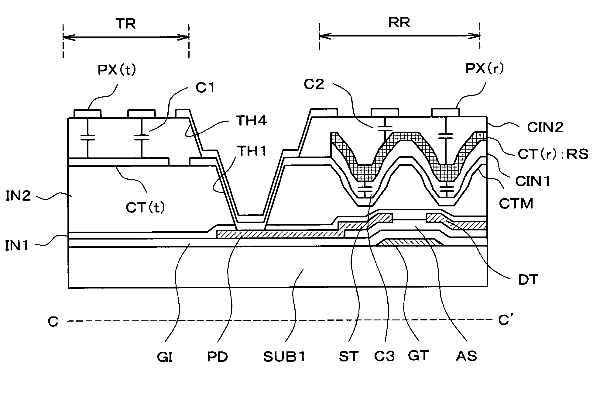
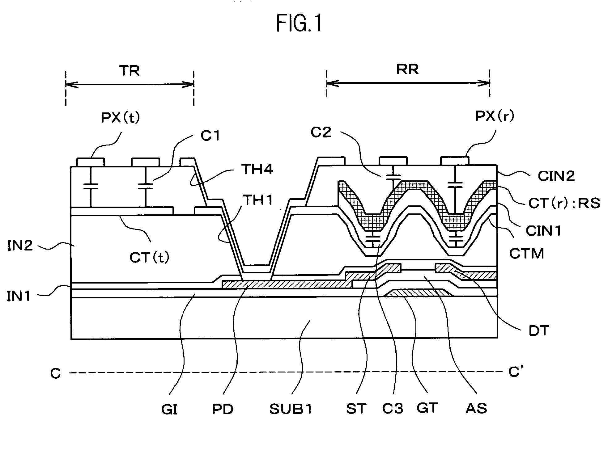
Liquid crystal display device
a display device and liquid crystal technology, applied in optics, instruments, electrical appliances, etc., can solve the problems of reducing contrast, inability to secure sufficient capacity, and difficulty in ensuring the flatness of the capacitor surface, so as to reduce the aperture ratio of the pixel, reduce the size of the storage capacity, and increase the storage capacity
- Summary
- Abstract
- Description
- Claims
- Application Information
AI Technical Summary
Benefits of technology
Problems solved by technology
Method used
Image
Examples
first preferred embodiment
[Overall Equivalent Circuit]
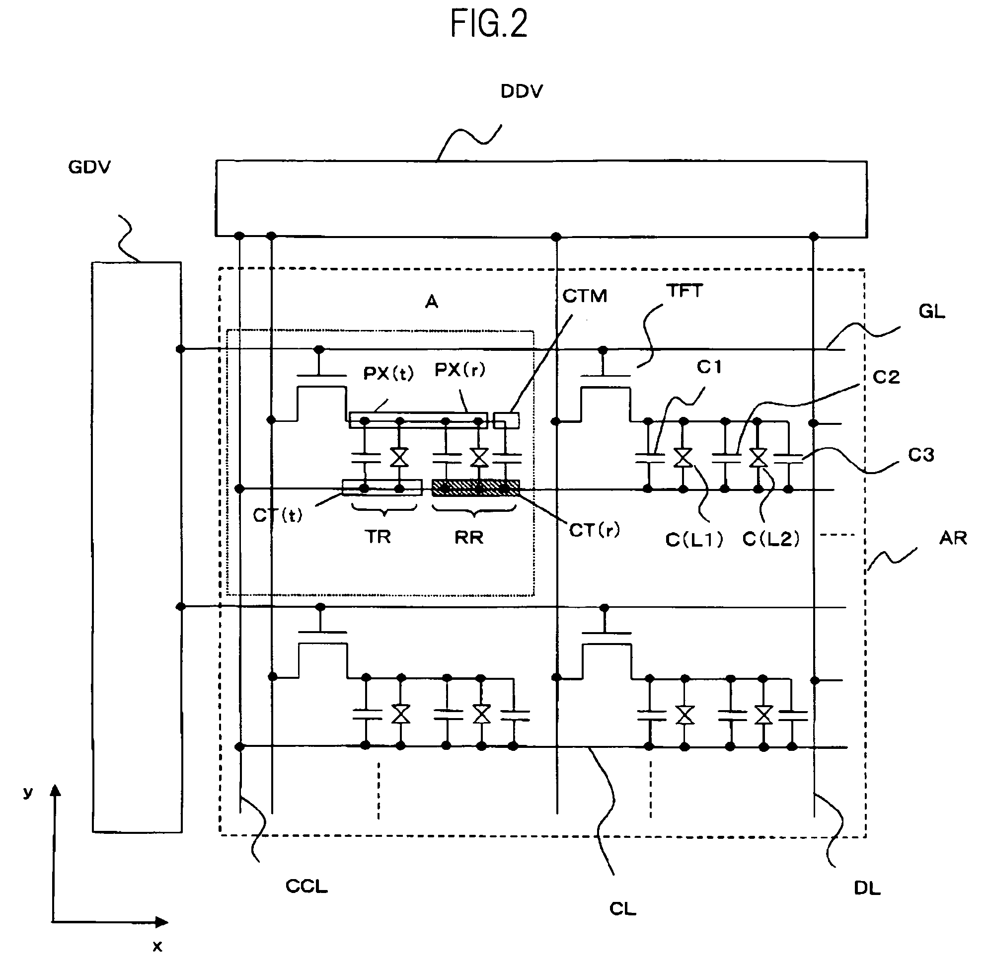
[0057]FIG. 2 is an equivalent circuit diagram of a liquid crystal display device according to various aspects of the present embodiment, which is called an IPS (In Plane Switching) liquid crystal display device. FIG. 2 is an equivalent circuit diagram formed over a surface, on the side near liquid crystal, of one substrate (shown with a reference SUB1) of a pair of substrates which are placed opposing each other with the liquid crystal therebetween. Although FIG. 2 is an equivalent circuit diagram, FIG. 2 also is drawn to correspond to the actual geometric placement.
[0058]In FIG. 2, first, gate signal lines GL which are formed extending in an x direction in FIG. 2 are formed aligned in a y direction in FIG. 2. Each of the gate signal lines GL is connected at the left end of FIG. 2 to a gate driver GDV. A scan signal is supplied to each gate signal line GL in a sequentially repeating manner by the gate driver GDV in the order, for example, from a gate sign...
second preferred embodiment
(Overall Equivalent Circuit)
[0152]FIG. 8 is an equivalent circuit diagram of a liquid crystal display device which is called a TN (Twisted Nematic) type or a VA (Vertical Alignment) type, and is drawn corresponding to FIG. 2. In FIG. 8, the members having the same reference numeral as FIG. 2 have the same functions.
[0153]The TN type or VA type liquid crystal display device has a structure in which an opposing electrode CT is provided over a surface of the substrate SUB2, which is placed opposing the substrate SUB1 with the liquid crystal therebetween, on the side near the liquid crystal. In FIG. 8, in addition to the circuits formed on the side of the substrate SUB1, the opposing electrode CT is also shown.
[0154]In FIG. 8, a structure different from the structure of FIG. 2 is that the pixel electrode PX connected to the source electrode ST of the thin film transistor TFT is formed with a transparent conductive film in the pixel electrode PX(t) formed in the transmissive region TR an...
PUM
| Property | Measurement | Unit |
|---|---|---|
| transparent | aaaaa | aaaaa |
| transparent conductive | aaaaa | aaaaa |
| voltage | aaaaa | aaaaa |
Abstract
Description
Claims
Application Information
 - R&D
- Intellectual Property
- Life Sciences
- Materials
- Tech Scout
- Unparalleled Data Quality
- Higher Quality Content
- 60% Fewer Hallucinations
Browse by: Latest US Patents, China's latest patents, Technical Efficacy Thesaurus, Application Domain, Technology Topic, Popular Technical Reports.
© 2025 PatSnap. All rights reserved.Legal|Privacy policy|Modern Slavery Act Transparency Statement|Sitemap|About US| Contact US: help@patsnap.com


