Organic electro-luminescence display device
a technology of electroluminescence display device and organic el, which is applied in the direction of discharge tube luminescnet screen, discharge tube/lamp details, organic semiconductor device, etc., can solve the problems of increasing the manufacturing cost of insufficient moisture capture effect, so as to prevent the reduction of light emission efficiency in the top-emission organic el display device. , the effect of simple process
- Summary
- Abstract
- Description
- Claims
- Application Information
AI Technical Summary
Benefits of technology
Problems solved by technology
Method used
Image
Examples
first preferred embodiment
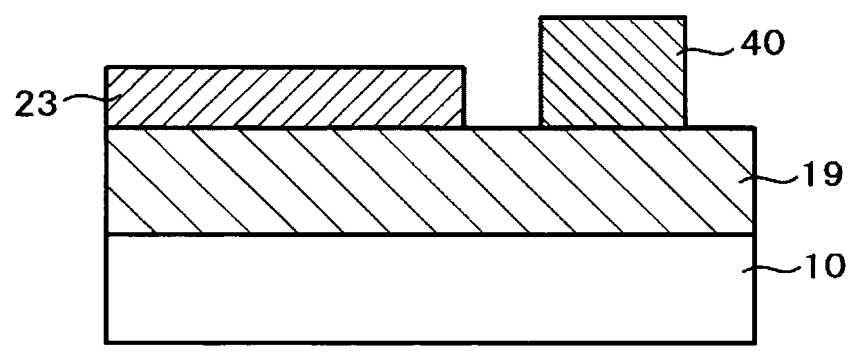
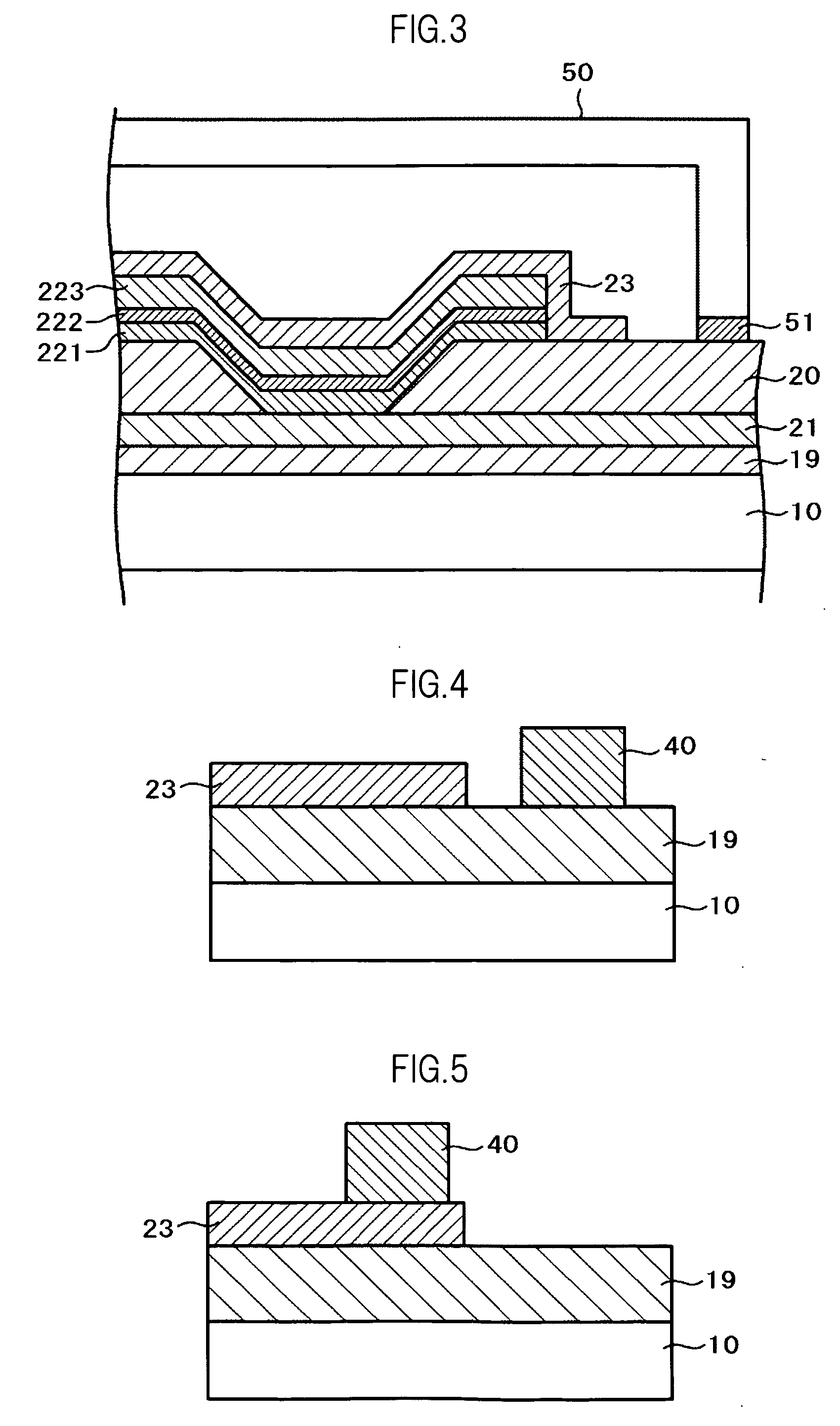
[0064]FIG. 4 is a cross sectional schematic view showing a first preferred embodiment of the present invention. In FIG. 4, the organic passivation film 19 is formed over the element substrate 10 comprising glass. The TFT, gate insulating film, interlayer insulating film, etc. which are formed below the organic passivation film 19 are not shown. The upper electrode 23 which functions as the anode is formed with IZO over the organic passivation film 19. The organic EL layer, lower electrode, etc. below the upper electrode 23 are not shown.
[0065]In the present embodiment, over the organic passivation film 19 in an area in which the upper electrode 23 is not present, a structure which uses the same materials as the electron transporting layer and has different constituent component is co-evaporated and is used as the desiccant 40. More specifically, the material is co-evaporation of an organic material and cesium as described above. As the desiccant 40, the composition of cesium is set ...
second preferred embodiment
[0071]FIG. 5 is a cross sectional schematic view showing a second preferred embodiment of the present invention. In FIG. 5, the organic passivation film 19 is formed over the element substrate 10 comprising glass. The elements formed below the organic passivation film 19 such as the TFT, gate insulating film, and interlayer insulating film are not shown. The upper electrode 23 which functions as the anode is formed with IZO over the organic passivation film 19. The elements below the upper electrode 23 such as the organic EL layer and the lower electrode are not shown.
[0072]In the present embodiment, the desiccant 40 by co-evaporation is formed over the upper electrode 23 in a region where the organic EL layer 22 is not present. Unlike the organic EL layer 22, the upper electrode 23 is evaporated in a pattern (so-called beta pattern) covering the entire surface of the element substrate 10 except for the terminal portion or the like. Therefore, the region where the upper electrode 23...
third preferred embodiment
[0074]FIG. 6 is a cross sectional schematic view of a third preferred embodiment of the present invention. In FIG. 6, the organic passivation film 19 is formed over the element substrate 10 comprising glass. The elements formed below the organic passivation film 19 such as the TFT, gate insulating film, and interlayer insulating film are not shown. The bank 20 for separating the pixels is formed with an acrylic resin over the organic passivation film 19. The upper electrode 23 by IZO extends over the bank 20.
[0075]In the present embodiment, both the upper electrode 23 and the bank 20 are covered with the desiccant 40 deposited by co-evaporation. The acrylic resin forming the bank 20 has a characteristic that it easily contains moisture. The moisture contained in the acrylic resin is released during a long-term operation of the organic EL display device and reduces the light emission efficiency of the organic EL layer 22, resulting in a black spot or the like.
[0076]In the present emb...
PUM
 Abstract
Description
Claims
Application Information
 - R&D
- Intellectual Property
- Life Sciences
- Materials
- Tech Scout
- Unparalleled Data Quality
- Higher Quality Content
- 60% Fewer Hallucinations
Browse by: Latest US Patents, China's latest patents, Technical Efficacy Thesaurus, Application Domain, Technology Topic, Popular Technical Reports.
© 2025 PatSnap. All rights reserved.Legal|Privacy policy|Modern Slavery Act Transparency Statement|Sitemap|About US| Contact US: help@patsnap.com


