
Method for fabricating spm and cd-spm nanoneedle probe using ion beam and spm and cd-spm nanoneedle probe thereby

Active Publication Date: 2009-04-23
KOREA RES INST OF STANDARDS & SCI
View PDF9 Cites 14 Cited by
  • Summary
  • Abstract
  • Description
  • Claims
  • Application Information

AI Technical Summary

Benefits of technology

[0016]Accordingly, it is an objective of the present invention to provide a method for fabricating a SPM nanoneedle probe capable of being easily adjusted with an intended pointing direction of a nanoneedle attached on a tip of the SPM nanoneedle probe and of being easily straightened with the nanoneedle attached on the tip of the SPM nanoneedle probe along the intended pointing direction, and to a SPM nanoneedle probe thereby.

Problems solved by technology

An SPM is a device used in a field of nanoscale technology, which is very powerful and useful as well as being delicate.
Because a conventional method which enhances an aspect ratio of a probe using semiconductor micromachining techniques has an inherent limitation in improving the resolution, a demand for an alternative method has been increased for sharpening the end of the probe.
However, the third factor remains unsolved by any methods disclosed so far.
However, Korean patent application 10-2002-0052591 still has technical disadvantages of long process time and high cost required to fabricate a nanoneedle SPM probe as well as low throughput because the patent application utilizes a nanomanipulator and a medium attached the tip of the probe to adjust the pointing direction of the nanoneedle.
Further, despite that the variation of the pointing direction of the nanoneedle attached on the tip of the SPM probe has to be within 2 to 3 degree to scan in critical dimension (CD), it is nearly impossible to adjust correctly the pointing direction of the nanoneedle with such an accuracy by the conventional technologies.
Besides, in some cases, the nanoneedle attached on the tip of the SPM probe is dither crooked or curled due to certain manufacturing problems.
Also, the conventional SPM probe or the SPM nanoneedle probe having an end with a shape of a straight line has a limitation in scanning the shape of the sidewall of the sample object having irregularity in nanoscale level.
Although U.S. Pat. No. 6,246,054 disclosed the SPM probe having an end with shapes illustrated in FIG. 15, it still has a disadvantage in that the method to fabricate such probe and the scanning method are too complicated.
Besides, it has a certain limitation in accuracy of the scanning the sidewall of a sample object to be scanned.

Method used


Image

  • Method for fabricating spm and cd-spm nanoneedle probe using ion beam and spm and cd-spm nanoneedle probe thereby
  • Method for fabricating spm and cd-spm nanoneedle probe using ion beam and spm and cd-spm nanoneedle probe thereby
  • Method for fabricating spm and cd-spm nanoneedle probe using ion beam and spm and cd-spm nanoneedle probe thereby

Examples


Embodiment Construction

[0039]Reference will now be made in detail to the aspects of the present invention, examples of which are illustrated in the accompanying drawings, wherein like reference numerals refer to like elements throughout. The aspects are described below in order to explain the present invention by referring to the figures.

[0040]As mentioned above, the term “nanoneedle” used hereinafter includes what terms “nanotube” and “nanowire” refer to. Also, the method of fabricating the SPM nanoneedle probe or the CD-SPM nanoneedle probe according to the present invention can be applied to all kinds of nanotube including a commonly used nanotube such as carbon nanotube, BCN nanotube, or BN nanotube, a single-walled nanotube, a double-walled nanotube, or a multi-walled nanotube, regardless of the kind of the nanotube.

[0041]Hereafter, preferred embodiments according to the present invention will be described in detail as examples in reference with the accompanying drawings.

[0042]As the prior patent doc...


PUM


Abstract

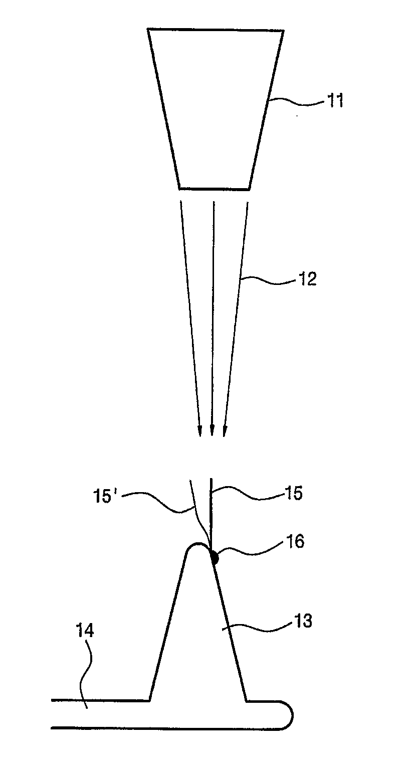
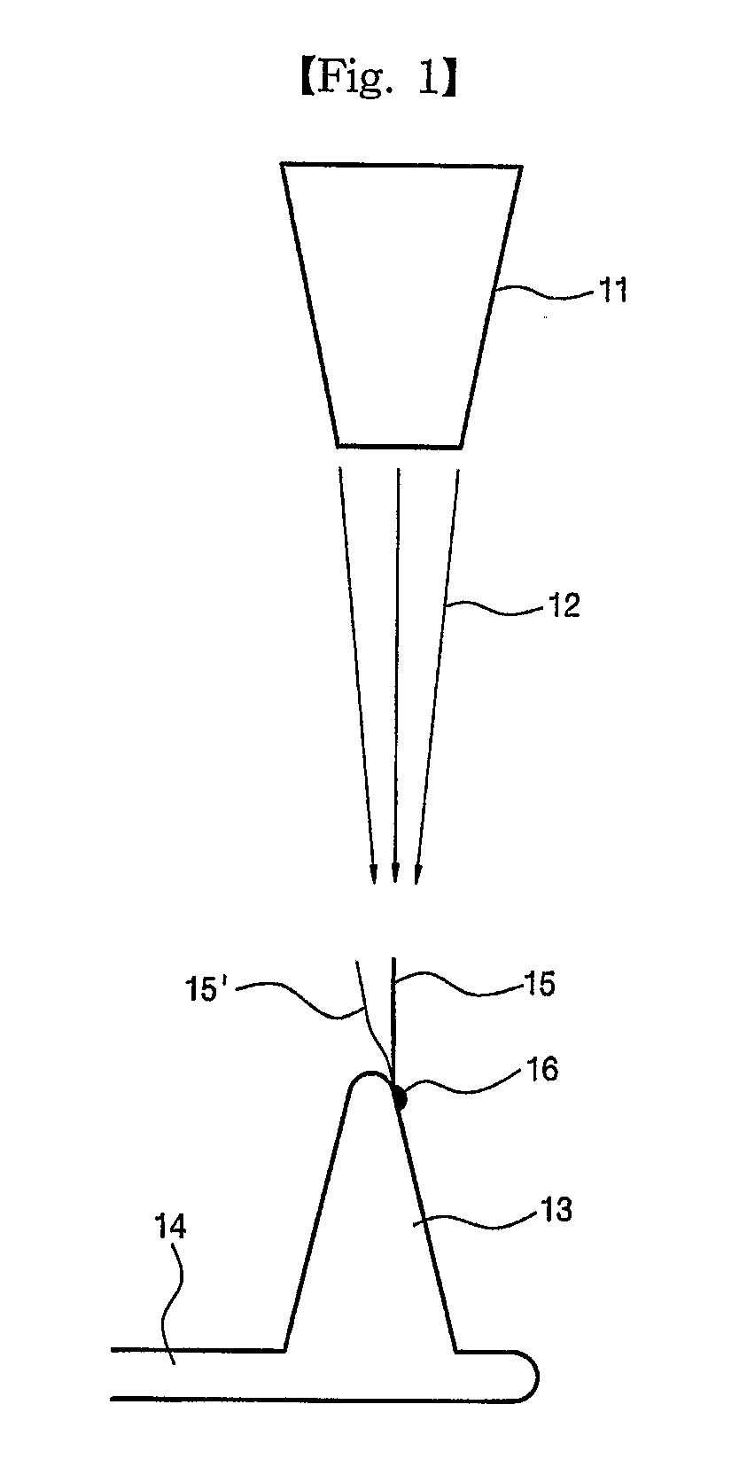
The present invention relates to a method for fabricating a scanning probe microscope (SPM) nanoneedle probe using ion beam which is preferably focused ion beam and a nanoneedle probe thereby. More particularly, the present invention relates to a method for fabricating a SPM nanoneedle probe capable of being easily adjusted with an intended pointing direction of a nanoneedle attached on a tip of the SPM nanoneedle probe and of being easily straightened with the nanoneedle attached on the tip of the SPM nanoneedle probe along the intended pointing direction, and to a SPM nanoneedle probe thereby. Also, the present invention relates to a method for fabricating a critical dimension SPM (CD-SPM) nanoneedle probe capable of precisely scanning the sidewall of an sample object in nanoscale using ion beam which is preferably focused ion beam, and to a CD-SPM nanoneedle probe thereby. More particularly, the present invention relates to a method for fabricating a CD-SPM nanoneedle probe capable of precisely scanning the sidewall of the sample object in nanoscale by bending a portion of an end of the nanoneedle attached on the tip of the SPM nanoneedle probe in a specific angle toward a direction other than an original direction in which the nanoneedle attached on the tip of the SPM nanoneedle probe extends out, and to a CD-SPM nanoneedle probe thereby. A method of fabricating scanning probe microscope (SPM) nanoneedle probe using ion beam, comprises: positioning the probe so that a tip of the probe on which the nanoneedle is attached faces toward a direction in which the ion beam is irradiated; and aligning the nanoneedle attached on the tip of the probe with the ion beam in parallel by irradiating the ion beam toward the tip of the probe on which the nanoneedle is attached. A method of fabricating a critical dimension scanning probe microscope (CD-SPM) nanoneedle probe using ion beam, comprises: screening a certain portion of the nanoneedle attached on a tip of the probe using a mask; and bending a part of the nanoneedle exposed out of the mask to align the part of the nanoneedle by irradiating the ion beam on the part of the nanoneedle exposed out of the mask, along the direction of the irradiated ion beam.

Description

TECHNICAL FIELD[0001]The present invention relates to a method for fabricating a scanning probe microscope (SPM) nanoneedle probe using an ion beam and a nanoneedle probe thereby. More particularly, the present invention relates to a method for fabricating a SPM nanoneedle probe capable of being easily adjusted with an intended pointing direction of a nanoneedle attached on a tip of the SPM nanoneedle probe and of being easily straightened with the nanoneedle attached on the tip of the SPM nanoneedle probe along the intended pointing direction, and to a SPM nanoneedle probe thereby.[0002]Also, the present invention relates to a method for fabricating a critical dimension SPM (CD-SPM) nanoneedle probe capable of precisely scanning the sidewall of an sample object in nanoscale using ion beam, and to a CD-SPM nanoneedle probe thereby. More particularly, the present invention relates to a method for fabricating a CD-SPM nanoneedle probe capable of precisely scanning the sidewall of the ...

Claims


Application Information

Patent Timeline
IPC IPC(8): G12B21/02G01Q70/16G01Q60/24G01Q60/38G01Q70/12
CPCB82Y15/00G01Q70/12G01Q60/38B82Y35/00A47C7/64
Inventor PARK, BYONG-CHEONJUNG, KI-YOUNGSONG, WON-YOUNGHONG, JAE-WANO, BEOM-HOANAHN, SANG-JUNG
Owner KOREA RES INST OF STANDARDS & SCI
Learn More