
Wiring board, semiconductor apparatus and method of manufacturing them

Active Publication Date: 2009-04-16
SHINKO ELECTRIC IND CO LTD
View PDF3 Cites 29 Cited by
  • Summary
  • Abstract
  • Description
  • Claims
  • Application Information

AI Technical Summary

Benefits of technology

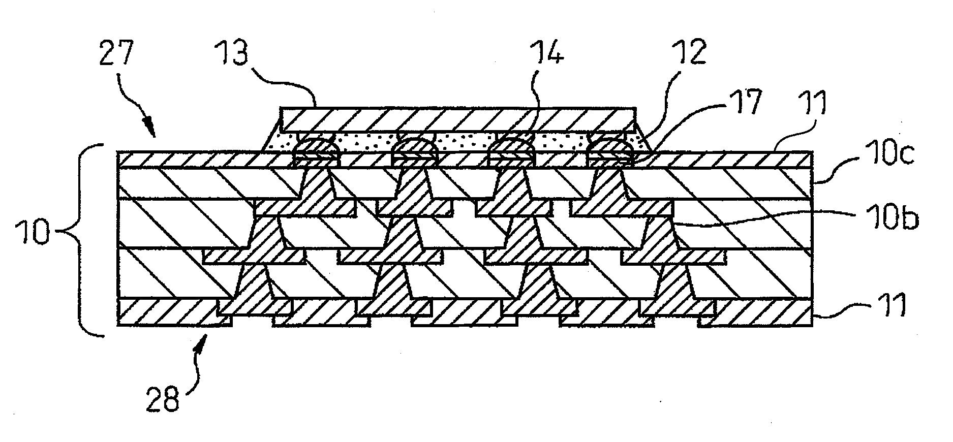
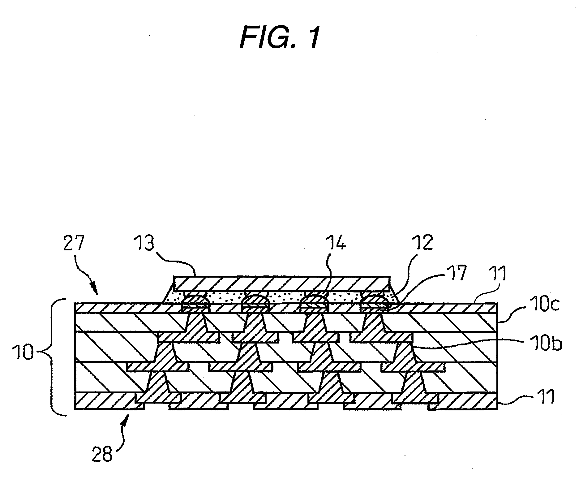
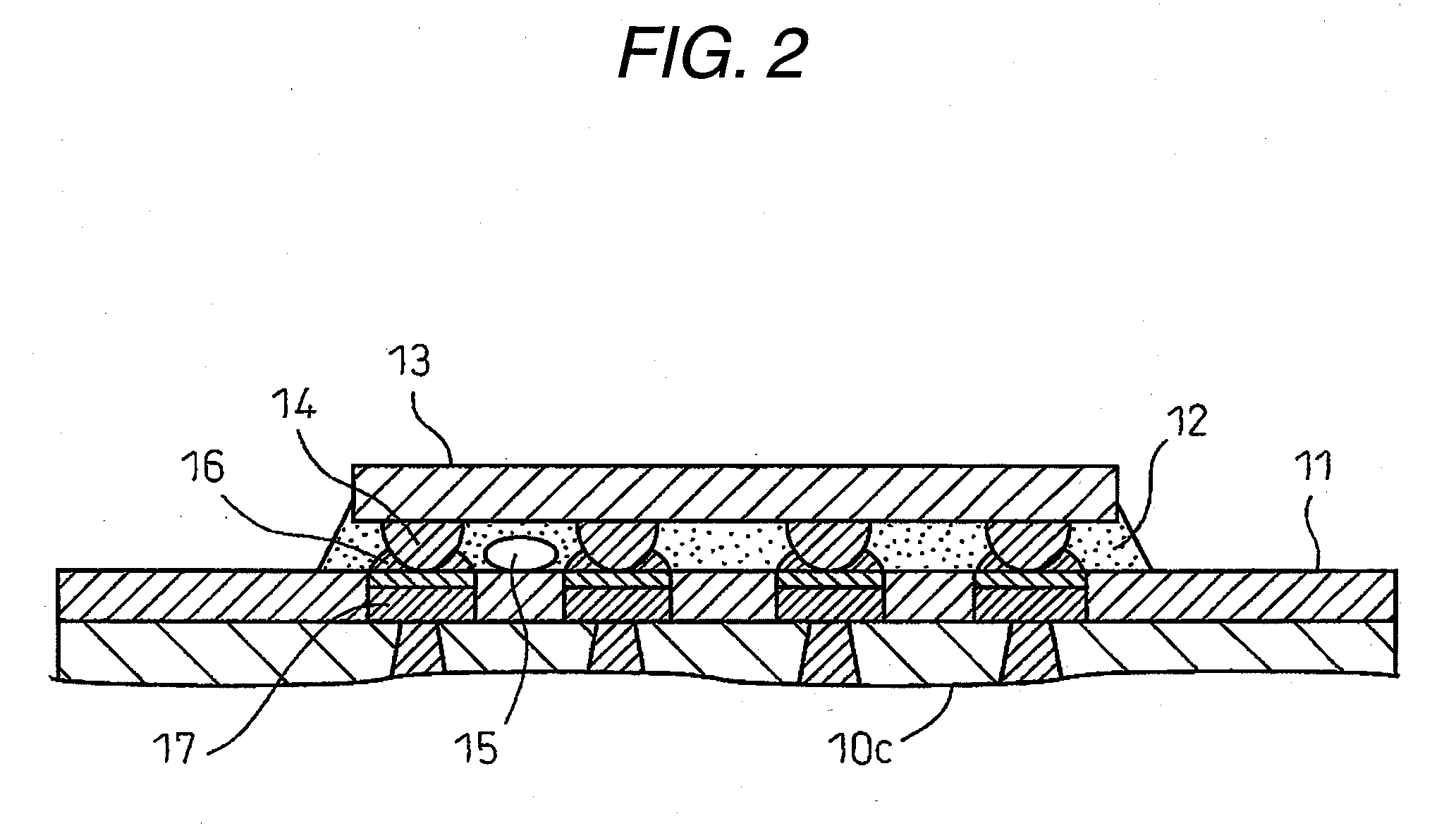
[0014]Exemplary embodiments of the present invention provide a method of manufacturing the wiring board and a semiconductor apparatus which can adjust a wettability between an underfill resin and an insulating layer or a solder resist layer which serves as a semiconductor device mounting surface by setting the semiconductor device mounting surface as a roughened surface, and particularly, can control a flowability of the underfill resin when filling the underfill resin, thereby forming the underfill resin well so as to prevent a void from being generated, and the wiring board and the semiconductor apparatus which are manufactured by the method.
[0015]Moreover, exemplary embodiments of the present invention a method of manufacturing a wiring board and a semiconductor apparatus which can enhance an adhesion between a support and an insulating layer or a solder resist layer in a manufacture and can prevent a generation of a defect such as sudden peeling of the support and the wiring board during the manufacture by setting, as a roughened surface, a surface of a support on which the wiring board (an intermediate body) is to be formed in the case in which the insulating layer and a wiring layer are provided on the support to form the wiring board, and the wiring board and the semiconductor apparatus which are manufactured by the method.
[0031]As described above, according to the invention, the roughening treatment is carried out before the dielectric layer or the wiring layer is formed on the surface of the support. Therefore, it is possible to adjust the wettability between the underfill resin and the insulating layer or the solder resist layer (that is, the dielectric layer). In particular, the flowability of the liquid underfill resin in filling of the underfill resin is controlled so that a void can be prevented from being generated in the underfill resin. Accordingly, it is possible to fill the underfill resin well between the semiconductor device and the wiring board.
[0032]By setting the surface of the support to be the roughened surface, moreover, it is possible to enhance an adhesion of the support and the insulating layer or the solder resist layer (the dielectric layer) during the manufacture. Consequently, it is possible to prevent the support and the wiring board from being suddenly peeled in the manufacture. Accordingly, it is possible to prevent a manufacturing defect of the wiring board or the semiconductor apparatus from being generated.

Problems solved by technology

Consequently, a defective appearance of a finished semiconductor package is generated.
In some cases in which the metal plate or the metal foil is used as the support and a surface of the wiring board from which the support is removed is set to be the semiconductor device mounting surface, therefore, the surface of the solder resist layer is excessively flat.
Accordingly, the wettability of the solder resist layer and the underfill resin is insufficient so that the void is generated in the underfill resin.

Method used


Image

  • Wiring board, semiconductor apparatus and method of manufacturing them
  • Wiring board, semiconductor apparatus and method of manufacturing them
  • Wiring board, semiconductor apparatus and method of manufacturing them

Examples


first embodiment

[0053]FIGS. 3A to 4D show a method of manufacturing a wiring board according to the invention in order of steps. In FIG. 3A, a support 20 is prepared. For the support 20, a metal plate formed of Cu or a metal foil formed of Cu in the same manner is generally used, for example. In case of a copper foil formed of Cu, a rolled copper foil or an electrolytic copper foil is suitably used.

[0054]A surface treatment for roughening a surface of the support 20 forming an insulating layer 23 is carried out at a subsequent step. Examples of a surface treatment include etching, oxidation, plating and blasting. As will be described below, in the examples according to the invention, there is carried out a so-called roughening treatment for carrying out soft etching (wet etching) by spraying an ammonium persulfate solution onto the surface of the support 20. FIG. 3B shows a surface 20a of the support 20 which is changed into a very small concavo-convex surface through the execution of the roughenin...

third embodiment

[0079]In the third embodiment, after the support 20 is subjected to the roughening treatment, the solder resist layer 29 is formed. Therefore, the solder resist layer 29 is buried in the roughened surface of the support 20, so that an adhesion between the solder resist layer 29 and the support 20 is improved. Further, the plating solution for the plated layer 22 does not flow into portions placed below the solder resist layer 29, and thus, the plated layer 22 with a stable shape can be formed. Further, since the adhesion between the solder resist layer 29 and the support 20 is improved, it is possible to prevent the intermediate body 40 and the support 20 from being peeled in the manufacturing process.

[0080]Further, in the first to third embodiments, after the roughened surface is formed on the support 20, the plated layer 22 (connecting pad) is formed. Therefore, it is possible to prevent the plated layer 22 from being damaged by etching, etc, due to the roughening treatment of the...


PUM

PropertyMeasurementUnit
Surface roughnessaaaaaaaaaa
Dielectric polarization enthalpyaaaaaaaaaa
Shapeaaaaaaaaaa

Abstract

There are provided steps of providing a dielectric layer and a wiring layer on a surface of a support to form an intermediate body, removing the support from the intermediate body to obtain a wiring board, and carrying out a roughening treatment over a surface of the support before the intermediate body forming step.

Description

TECHNICAL FIELD[0001]The present disclosure relates to a wiring board to be used in a semiconductor apparatus or a semiconductor package and a method of manufacturing the wiring board. More particularly, the present disclosure relates to a wiring board formed by using a support for a reinforcement in a manufacturing process to provide an insulating layer and a wiring layer on the support through a build-up method and then removing the support and a method of manufacturing the wiring board. Furthermore, the present disclosure relates to a semiconductor apparatus formed by using a wiring board formed through the same method and a method of manufacturing the semiconductor apparatus.RELATED ART[0002]A support is used for a reinforcement in a manufacture of a wiring board. As the related art of the case in which the wiring board is thus manufactured by using the support, there has been known a method of manufacturing a wiring board in which a dielectric layer (an insulating layer or a so...

Claims


Application Information

Patent Timeline
IPC IPC(8): H05K1/00H05K3/36H05K1/11H05K1/16
CPCH01L23/3121Y10T29/49126H01L23/3142H01L2924/01079H01L2224/16H05K2203/1152H05K3/28H01L2224/32225H01L21/563H01L2924/01019H05K3/205H01L2224/73204H01L21/6835H05K2201/10674H01L24/48Y10T29/4916H05K3/381H01L2924/01046H01L2224/32057Y10T29/41H05K2203/0152H01L2924/01078H01L2924/0102H01L2224/83385H01L2224/48091H05K3/4682H01L2221/68345H05K3/382H01L24/16H01L2924/00014H01L2224/16225H01L2924/15174H01L2924/181H01L2924/00012H01L2224/45099H01L2224/45015H01L2924/207H01L2924/00
Inventor KANEKO, KENTARO
Owner SHINKO ELECTRIC IND CO LTD
Learn More