
Validation Of An Integrated Circuit For Electro Static Discharge Compliance

a technology of electro static discharge and integrated circuit, which is applied in the field of software tools used in computer aided design (cad) of integrated circuits, can solve the problems of high current flow, general undesirable esd, and damage to various functional circuits within the i

Active Publication Date: 2009-04-09
TEXAS INSTR INC
View PDF11 Cites 17 Cited by
  • Summary
  • Abstract
  • Description
  • Claims
  • Application Information

AI Technical Summary

Problems solved by technology

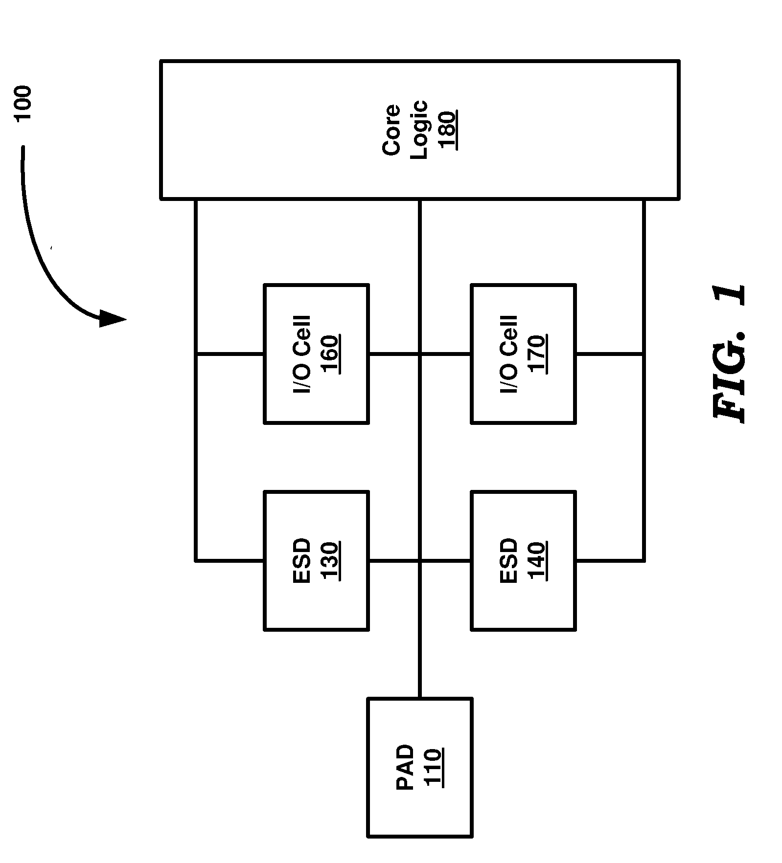
ESD is generally undesirable in that the magnitude of the current is often much higher than the magnitude for which an IC may be designed for during normal use in systems / devices.
Such high current flow can damage various functional circuits within an IC, as is well known in the relevant arts.

Method used


Image

  • Validation Of An Integrated Circuit For Electro Static Discharge Compliance
  • Validation Of An Integrated Circuit For Electro Static Discharge Compliance
  • Validation Of An Integrated Circuit For Electro Static Discharge Compliance

Examples


Embodiment Construction

1. Overview

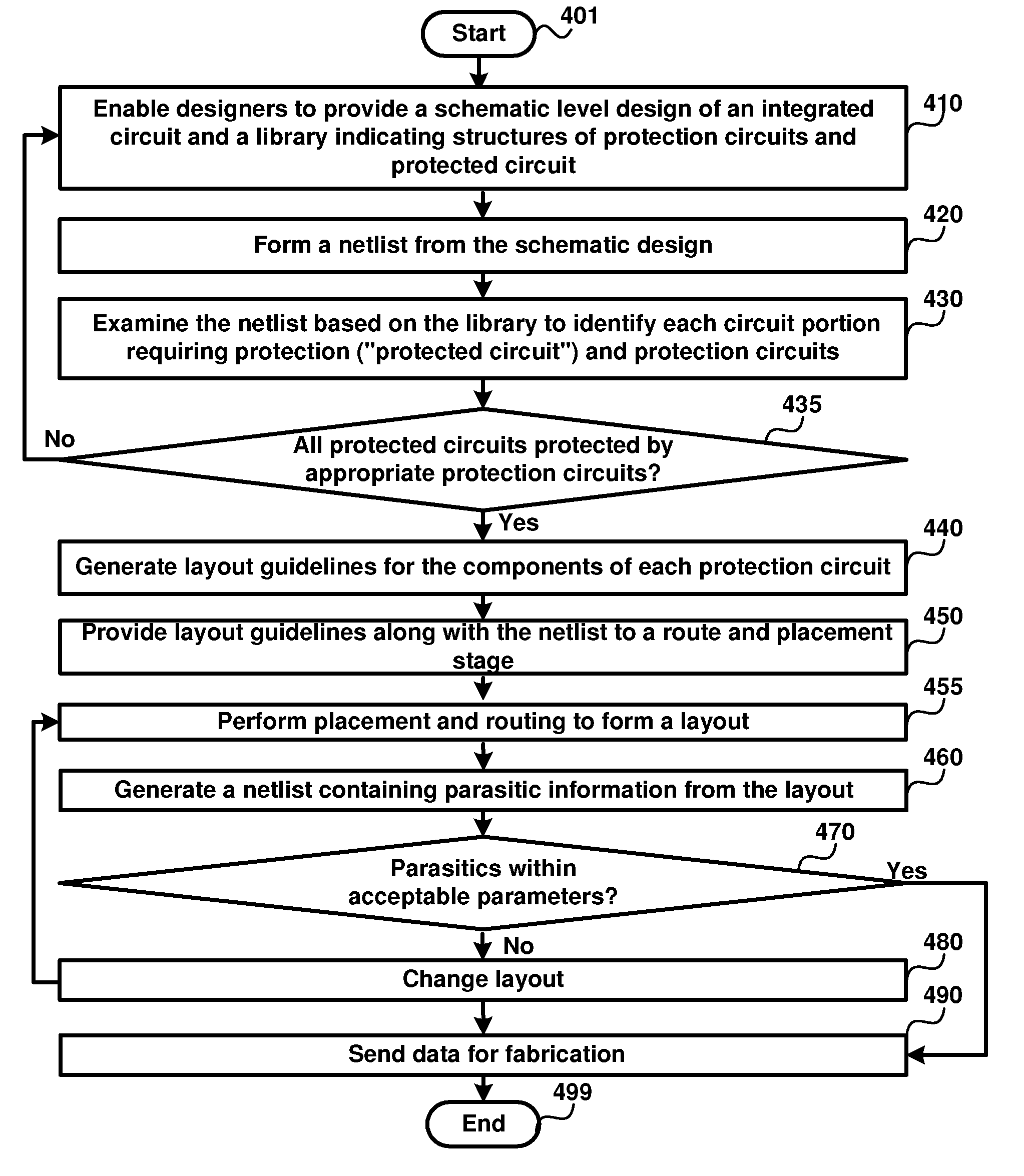
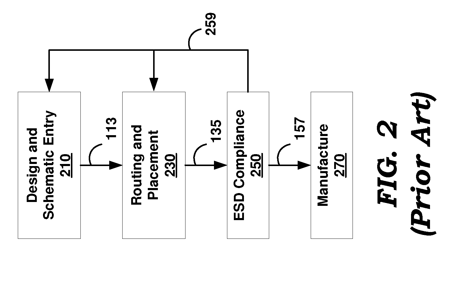
[0018]An aspect of the present invention validates ESD compliance by examining netlist data generated from a schematic level design of an integrated circuit. Routing and placement may be performed only after confirming that whether each protected circuit (having exposure to ESD current, without the protection circuit) is protected by an appropriate protection circuit. As a result, the design cycle time may be reduced.

[0019]According to another aspect of the present invention, layout guidelines for each protection circuit is also considered in performing the routing and placement. As a result, the number of iterations in a design cycle may be reduced.

[0020]According to yet another aspect of the present invention, another netlist may be extracted from layout information (generated by routing and placement), with the another netlist including parasitic information between nodes of a protection circuit. The acceptability of the parasitic may also thus be verified at the netli...


PUM


Abstract

An aspect of the present invention validates ESD compliance by examining netlist data generated from a schematic level design of an integrated circuit. Routing and placement may be performed only after confirming that whether each protected circuit (having exposure to ESD current, without the protection circuit) is protected by an appropriate protection circuit. As a result, the design cycle time may be reduced. According to another aspect of the present invention, layout guidelines for each protection circuit is also considered in performing the routing and placement. As a result, the number of iterations in a design cycle may be reduced.

Description

BACKGROUND[0001]1. Field[0002]The present disclosure relates software tools used in computer aided design (CAD) of integrated circuits, and more specifically to a method and apparatus for validating integrated circuits for electro static discharge (ESD) compliance.[0003]2. Related Art[0004]Electro static discharge (ESD) generally refers to the flow of electric charges (current) through the interface pads of an integrated circuit (IC), typically while not in use. One example of such not-in-use scenario is while packages containing the ICs are transported / moved prior to deployment in corresponding systems / devices. A common reason for the ESD is interface pads coming in contact with human beings while being deployed on systems or during transportation.[0005]ESD is generally undesirable in that the magnitude of the current is often much higher than the magnitude for which an IC may be designed for during normal use in systems / devices. Such high current flow can damage various functional...

Claims


Application Information

Patent Timeline
IPC IPC(8): G06F17/50
CPCG06F2217/12G06F17/5081G06F30/398G06F2119/18Y02P90/02
Inventor SHUKLA, VRASHANK GURUDATTAHOMACK, JAMES GARRETTKUNZ, JOHN ERIC
Owner TEXAS INSTR INC
Learn More