Method to improve transistor tox using si recessing with no additional masking steps

a transistor and recessing technology, applied in the direction of semiconductor devices, basic electric elements, electrical appliances, etc., can solve the problems of poor activation level in the crystalline, undetected punching through and/or leakage, and overrun of the extension regions, so as to reduce the defect of threading dislocation

Active Publication Date: 2009-04-09
TEXAS INSTR INC
View PDF9 Cites 15 Cited by
  • Summary
  • Abstract
  • Description
  • Claims
  • Application Information

AI Technical Summary

Benefits of technology

[0009]In one example, the silicon germanium material is doped with boron in-situ for the formation of p-type extension regions. In another example, an extension region implant is performed into the silicon germanium material after the selective epi deposition, followed by the formation of sidewall spacers and source/drain impl...

Problems solved by technology

However, too much doping in the source/drain regions can lead to overrun of the extension regions, and lead undesirably to punchthrough and/or leakage.
The excellent abruptness of SPER junction results from a poor activation level in the crystalline Si below the amorphous region...

Method used


Image

  • Method to improve transistor tox using si recessing with no additional masking steps
  • Method to improve transistor tox using si recessing with no additional masking steps
  • Method to improve transistor tox using si recessing with no additional masking steps

Examples


Embodiment Construction

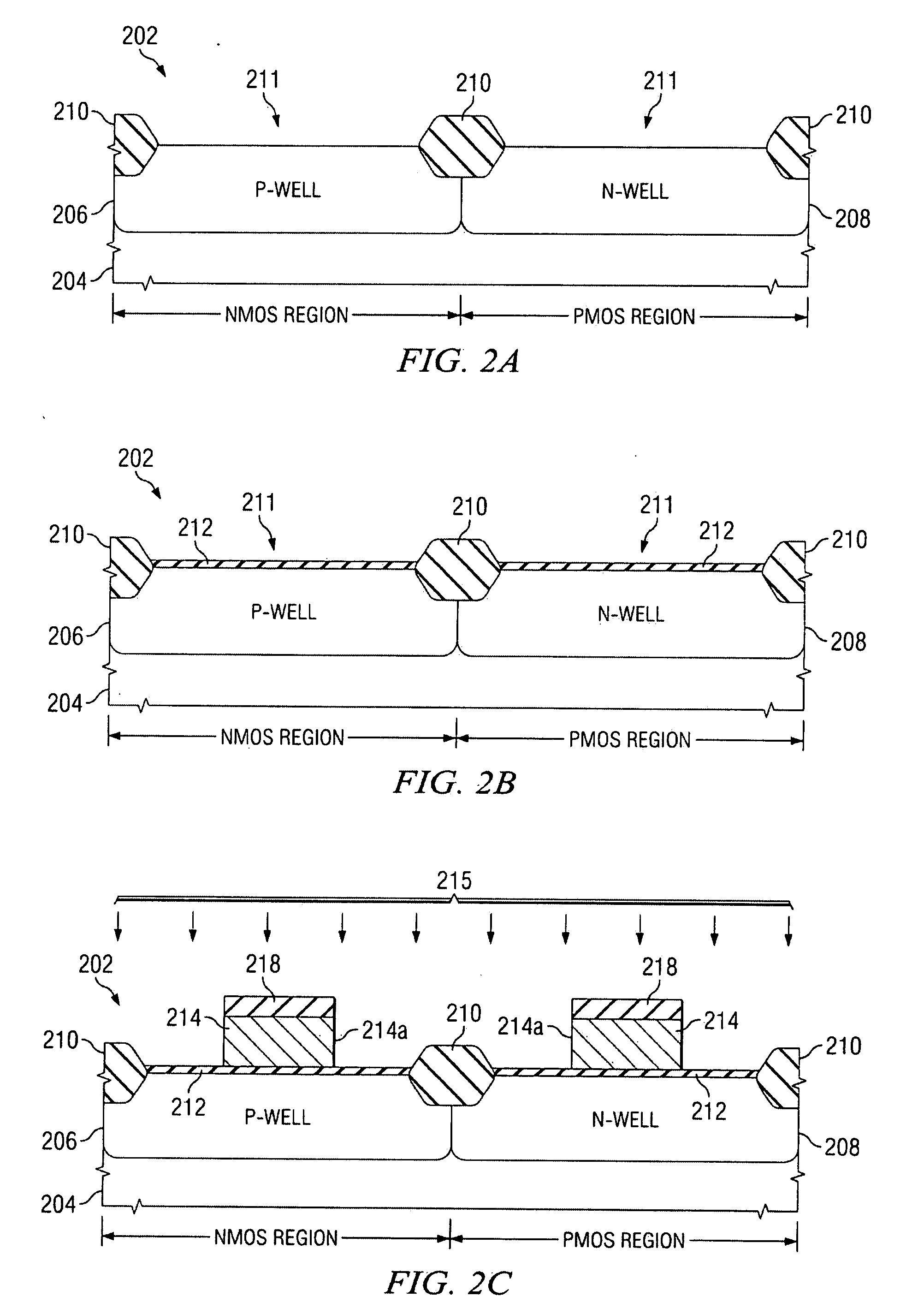
[0019]One or more implementations of the present invention will now be described with reference to the attached drawings, wherein like reference numerals are used to refer to like elements throughout, and wherein the illustrated structures are not necessarily drawn to scale. The invention provides transistor structures and methods in which transistor mobility is improved while minimizing defects heretofore associated with conventional strained silicon device solutions.

[0020]Referring now to FIGS. 1 and 2A-2J, further aspects of the invention relate to methods of fabricating integrated circuits, wherein FIG. 1 illustrates an exemplary method 100 in accordance with the invention, and FIGS. 2A-2J illustrate the exemplary transistor device at various stages of fabrication in accordance with the invention. While the exemplary method 100 is illustrated and described below as a series of acts or events, it will be appreciated that the present invention is not limited by the illustrated ord...


PUM


Abstract

A method of forming a transistor device is provided wherein a gate structure is formed over a semiconductor body of a first conductivity type. The gate structure is formed comprising a protective cap thereover and defining source/drain regions laterally adjacent thereto. A first implant is performed of a second conductivity type into both the gate structure and the source/drain regions. The semiconductor body is etched to form recesses substantially aligned to the gate structure wherein the first implant is removed from the source/drain regions. Source/drain regions are implanted or grown by a selective epitaxial growth.

Description

FIELD OF THE INVENTION[0001]The present invention relates to various methods for the manufacture of transistor devices to improve poly depletion and oxide thickness.BACKGROUND OF THE INVENTION[0002]Field effect transistors (FETs) are widely used in the electronics industry for switching, amplification, filtering, and other tasks related to both analog and digital electrical signals. Most common among these are metal-oxide-semiconductor field-effect transistors (MOSFETs), wherein a gate electrode is energized to create an electric field in a channel region of a semiconductor body, by which electrons are allowed to travel through the channel between a source region and a drain region of the semiconductor body. The source and drain regions are typically formed by adding dopants to targeted regions on either side of the channel. A gate dielectric or gate oxide is formed over the channel, and a gate electrode or gate contact is formed over the gate dielectric. The gate dielectric and gat...

Claims


Application Information

Patent Timeline
IPC IPC(8): H01L21/8238H01L21/336
CPCH01L21/823807H01L29/7848H01L21/823842H01L21/823814
Inventor OBRADOVIC, BORNAEKBOTE, SHASHANK S.
Owner TEXAS INSTR INC
Why Eureka
Try Eureka