Electrically Conductive Material
a technology of electrical conductivity and material, applied in the field of electrical conductivity materials, can solve the problems of insufficient improvement and increase of resistivity of semiconductor devices
- Summary
- Abstract
- Description
- Claims
- Application Information
AI Technical Summary
Benefits of technology
Problems solved by technology
Method used
Image
Examples
example 1 (
E1)
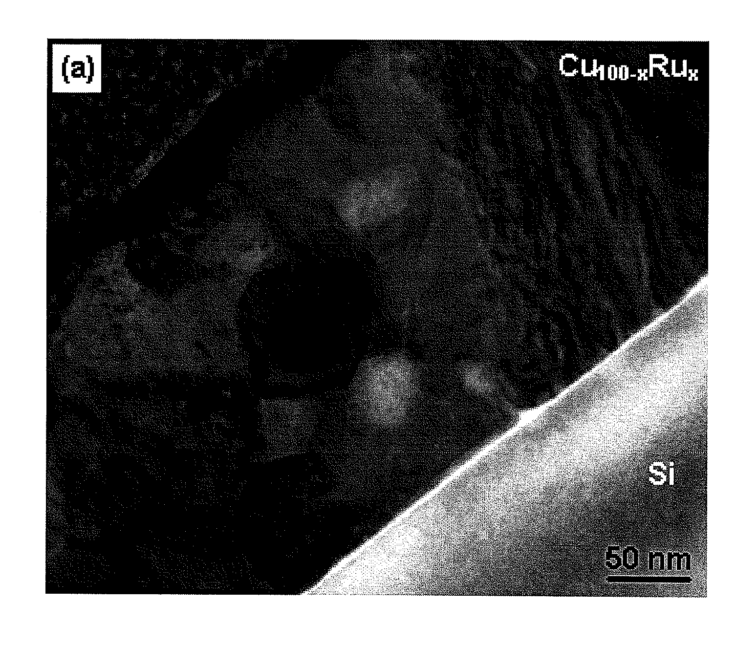
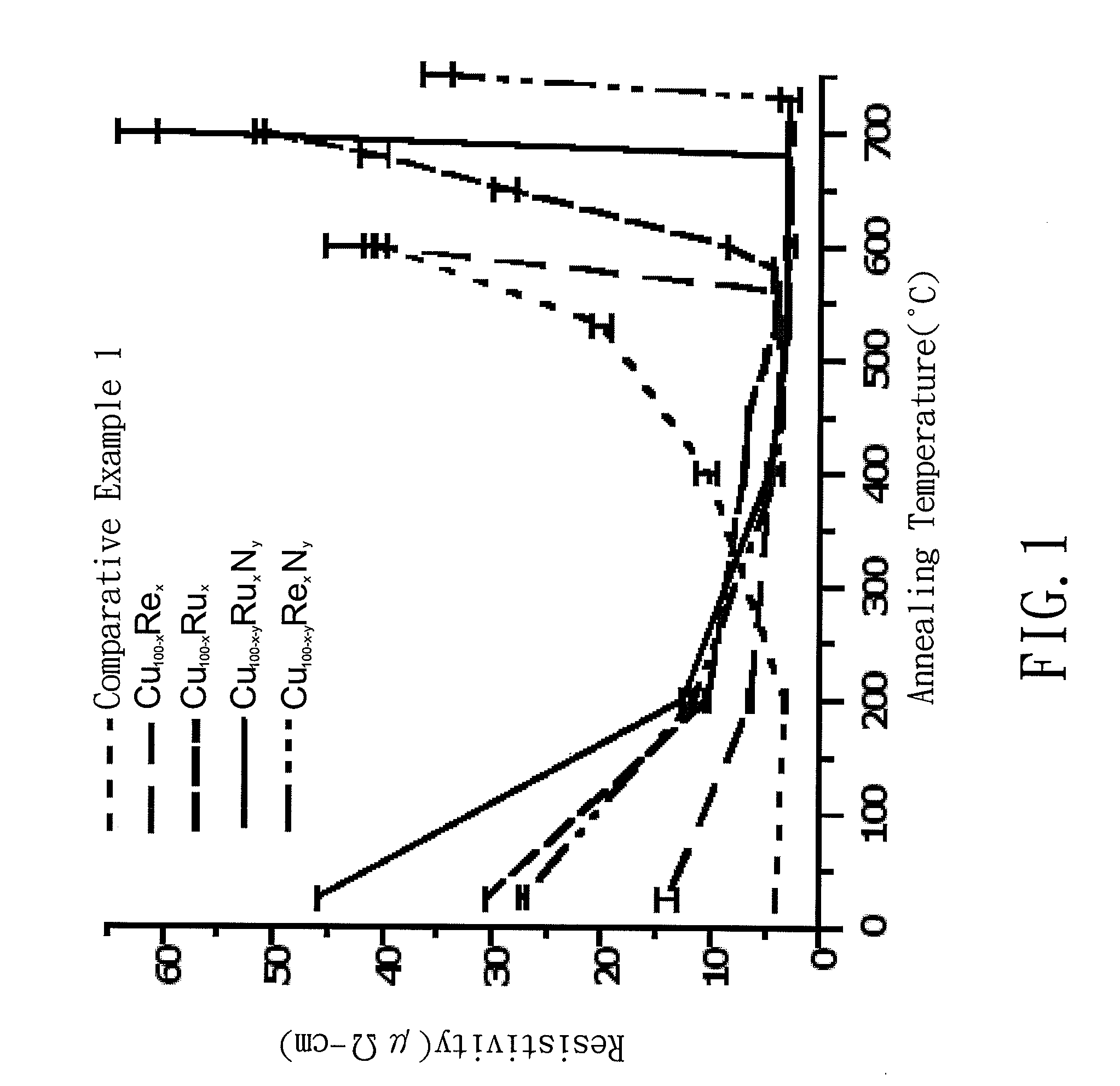
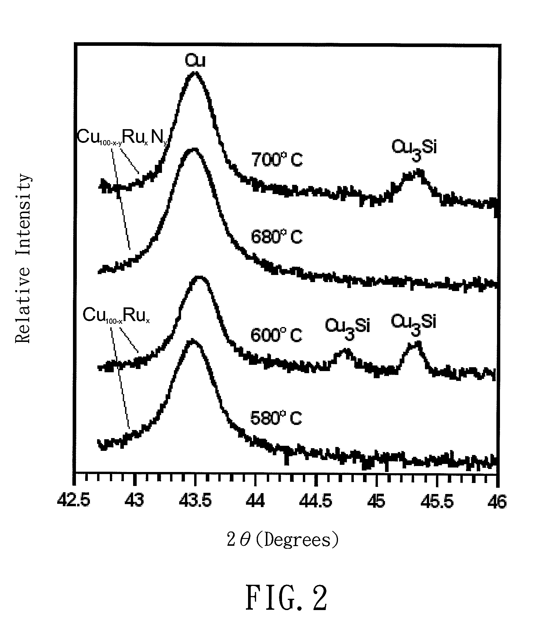
[0035]A Si substrate was placed inside a magnetron sputtering system. A feed gas including argon plasma was introduced into the sputtering system under a working pressure of 1×10⁻² torr. After applying an output power of 150 W on a Cu—Ru target, a Cu100-xRux film, x=0.6, was formed on the Si substrate and had a thickness of approximately 300 nm. The sputtering operation was conducted at a sputtering rate of 4.8 nm / min. The temperature of the Si substrate was approximately 80° C. during the deposition of the Cu100-xRux film. Subsequently, specimens of the Cu100-xRux film thus formed were subjected to annealing treatment so as to eliminate residual stress therein and so as to enable Ru to precipitate from copper lattice sites and into copper grain boundaries. The annealing temperatures for the corresponding specimens were 200° C., 400° C., 580° C. and 600° C., respectively (see FIG. 1). A Pt film was then formed on each specimen of the Cu100-xRux film for microscope measurement.
example 2 (
E2)
[0036]The polycrystalline copper alloy of Example 2 was prepared using steps similar to those of Example 1, except that the feed gas included argon and nitrogen plasma. The polycrystalline copper alloy thus formed was Cu100-x-yRuxNy, wherein x=0.4, and y=1.7. Subsequently, specimens of the Cu100-x-yRuxNy film thus formed were subjected to annealing treatment. The annealing temperatures for the corresponding specimens were 200° C., 400° C., 680° C. and 700° C. respectively (see FIG. 1).
example 3 (
E3)
[0037]The polycrystalline copper alloy of Example 3 was prepared using steps similar to those of Example 1, except that the target employed in the sputtering system was Cu—Re. The polycrystalline copper alloy thus formed was Cu100-xRex, wherein x=0.9. Subsequently, specimens of the Cu100-xRex film thus formed were subjected to annealing treatment. The annealing temperatures for the corresponding specimens were 200° C., 400° C., 560° C. and 580° C., respectively (see FIG. 1).
PUM
| Property | Measurement | Unit |
|---|---|---|
| Grain size | aaaaa | aaaaa |
| Grain size | aaaaa | aaaaa |
| Temperature | aaaaa | aaaaa |
Abstract
Description
Claims
Application Information
 - R&D
- Intellectual Property
- Life Sciences
- Materials
- Tech Scout
- Unparalleled Data Quality
- Higher Quality Content
- 60% Fewer Hallucinations
Browse by: Latest US Patents, China's latest patents, Technical Efficacy Thesaurus, Application Domain, Technology Topic, Popular Technical Reports.
© 2025 PatSnap. All rights reserved.Legal|Privacy policy|Modern Slavery Act Transparency Statement|Sitemap|About US| Contact US: help@patsnap.com


