Adhesion composition, making method of adhesion composition, display device and making method of display device
a technology of adhesion composition and adhesive composition, which is applied in the direction of instruments, cellulosic plastic layered products, synthetic resin layered products, etc., can solve the problems of contaminating the liquid crystal layer, the optical property of the lcd device will not be consistent as well, and the cell gap may not be consistent if the lcd device, so as to achieve the effect of appropriate strength and not easily deformed
- Summary
- Abstract
- Description
- Claims
- Application Information
AI Technical Summary
Benefits of technology
Problems solved by technology
Method used
Image
Examples
first embodiment
[0052]A liquid crystal display device according to the present invention will be described with reference to FIGS. 1 to 3.
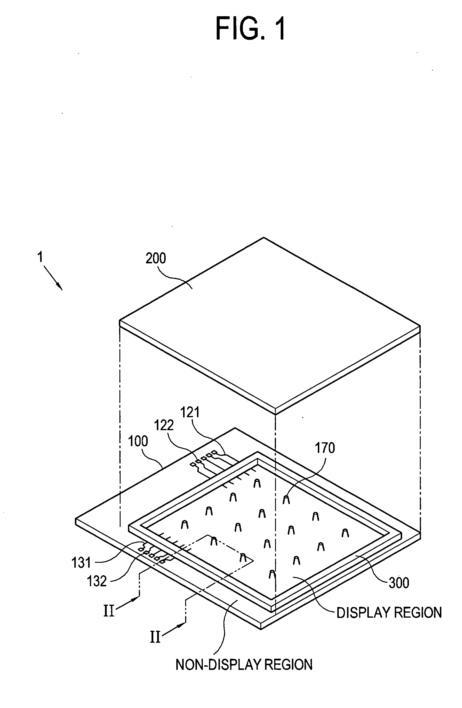
[0053]As shown in FIG. 1, a liquid crystal display device 1 includes a first substrate 100, a second substrate 200, and a sealant 300. FIG. 1 does not illustrate a liquid crystal layer 400 and an adhesion layer 500 (refer to FIG. 2) for convenience.
[0054]The first substrate 100 is larger than the second substrate 200. The internal part of the sealant 300 corresponds to a display region while the external part corresponds to a non-display region. The first substrate 100 includes a gate line 121 extending to the display region, a gate pad 122 connected with the gate line 121 and disposed in the non-display region, a data line 131 extending to the display region, and a data pad 132 connected with the data line 131 and disposed in the non-display region.
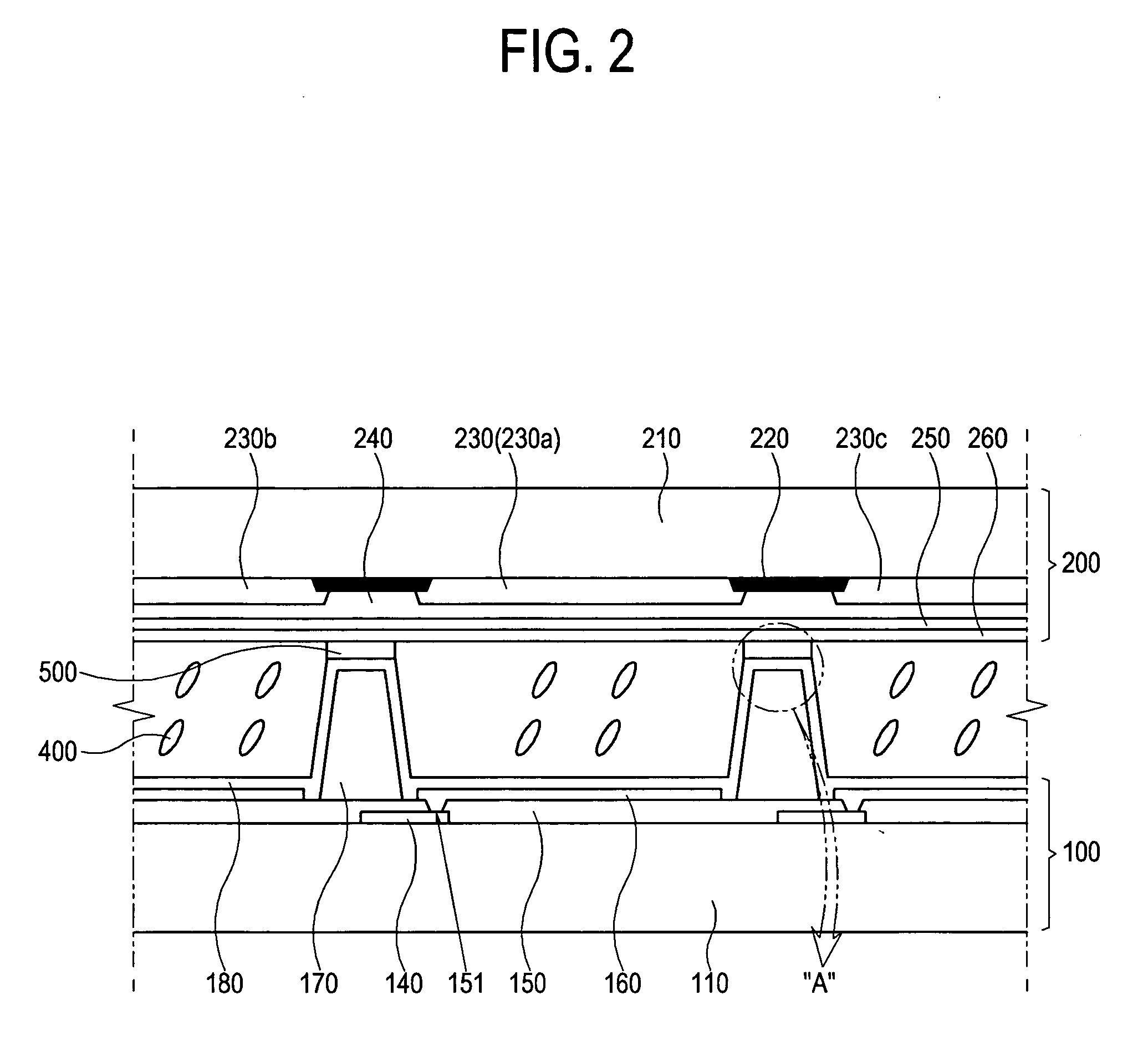
[0055]The gate line 121 and the data line 131 are connected with a thin film transistor (TFT) 140 (refer to FIG. 2)...
second embodiment
[0131]Referring to FIG. 12, a liquid crystal display device 2 according to the present invention will be described.
[0132]A pixel electrode cutting pattern 161 is formed in a pixel electrode 160 while a common electrode cutting pattern 251 is formed in a common electrode 250. The liquid crystal molecule of a liquid crystal layer 400 has negative dielectric anisotropy. A longer axis of the liquid crystal molecule is vertically aligned to an electric field.
[0133]First and second alignment layers 180 and 260 are vertical alignment layers, and the longer axis of the liquid crystal molecule is vertically aligned to first and second substrates 100 and 200 while the electric field is not formed. The liquid crystal layer 400 contacts both the first and second alignment layers 180 and 260, and is initially aligned without difficulty.
[0134]If the electric field is formed between the pixel electrode 160 and the common electrode 250, the longer axis of the liquid crystal molecule is horizontally...
PUM
| Property | Measurement | Unit |
|---|---|---|
| Temperature | aaaaa | aaaaa |
| Temperature | aaaaa | aaaaa |
| Temperature | aaaaa | aaaaa |
Abstract
Description
Claims
Application Information
 - R&D
- Intellectual Property
- Life Sciences
- Materials
- Tech Scout
- Unparalleled Data Quality
- Higher Quality Content
- 60% Fewer Hallucinations
Browse by: Latest US Patents, China's latest patents, Technical Efficacy Thesaurus, Application Domain, Technology Topic, Popular Technical Reports.
© 2025 PatSnap. All rights reserved.Legal|Privacy policy|Modern Slavery Act Transparency Statement|Sitemap|About US| Contact US: help@patsnap.com


