Wafer Working Method

a working method and wafer technology, applied in the field of wafer working methods, can solve the problems of inability to handle as a wafer, the wafer is undesired to be broken up from the inside modified region, and the number of defective chips produced

Inactive Publication Date: 2009-01-08
TOKYO SEIMITSU
View PDF7 Cites 26 Cited by
  • Summary
  • Abstract
  • Description
  • Claims
  • Application Information

AI Technical Summary

Benefits of technology

[0020]The present invention has been made in view of the foregoing problems and, accordingly, an object of the present invention is to provide a wafer working method capable of working a wafer diced by the laser dicing apparatus without causing any defect.

Problems solved by technology

The conventional chip fabrication method, however, involves a problem that when a very thin wafer W having a thickness of not more than 100 μm is subjected to cutting by dicing saw, a number of defective chips are produced due to chipping or cracking of the wafer W that occurs at the time of cutting.
Also, since the laser dicing apparatus does not have any portion to contact the wafer directly and hence does not allow heat or cutting swarf to be produced, no cutting water is needed.
With such a laser dicing apparatus, however, in some cases the wafer is undesirably broken up from the inside modified region as a starting point by impact or vibration that occurs during conveyance between apparatuses used in respective steps performed after dicing.
The wafer, once broken up, cannot be handled as a wafer, which raises a problem that the subsequent steps are seriously hindered from proceeding.
In this process, however, there has been observed in the second machining a phenomenon that due to the mechanical strength of the wafer lowered by the modified region, chipping occurs at a peripheral portion of the wafer and the resulting chipping is caught between a grinding wheel and the wafer to cause a scratch or caught between a polishing pad and the wafer to cause a flaw.
When such chipping is large, a notch portion or an orientation flat portion of the wafer may be damaged to give rise to an inconvenience in wafer alignment.

Method used


Image

  • Wafer Working Method
  • Wafer Working Method
  • Wafer Working Method

Examples


Embodiment Construction

[0051]Hereinafter, preferred embodiments of a wafer working method according to the present invention will be described in detail with reference to the attached drawings.

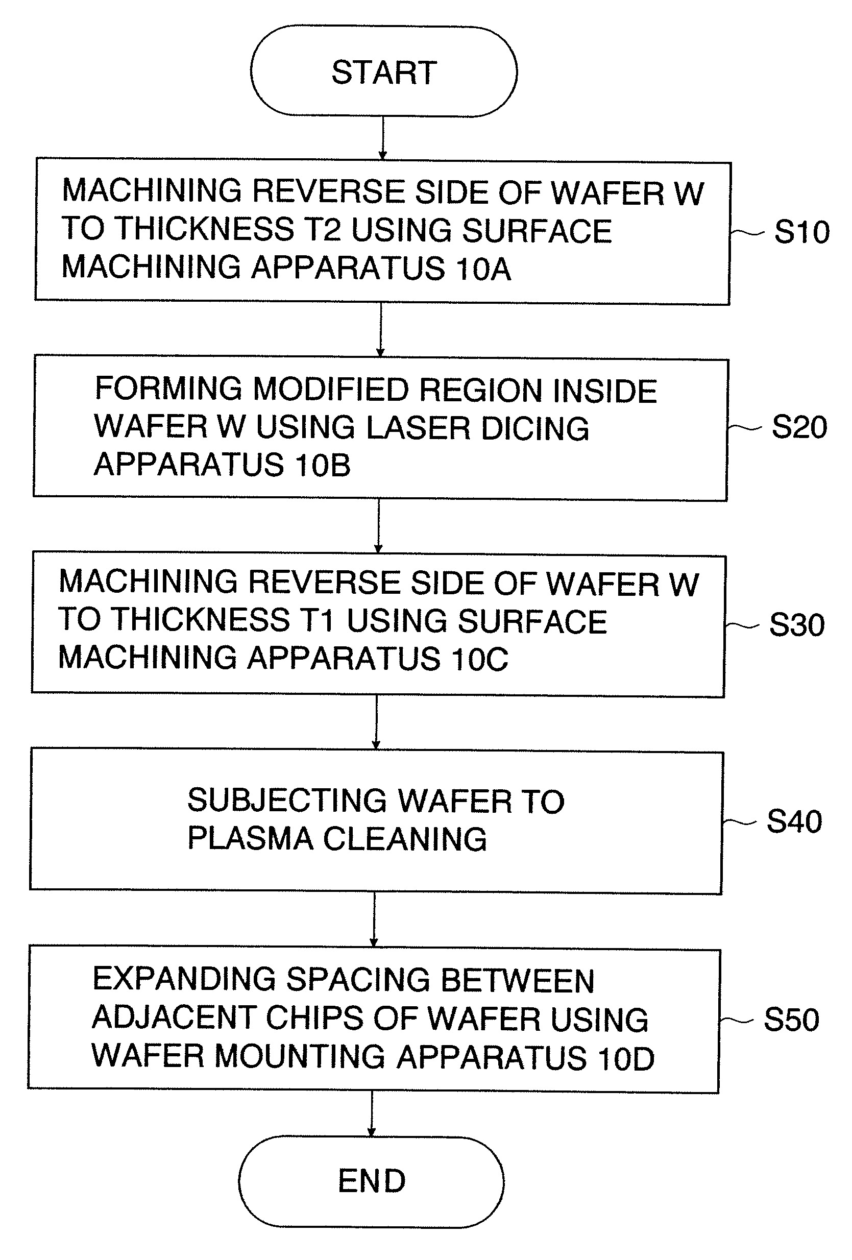
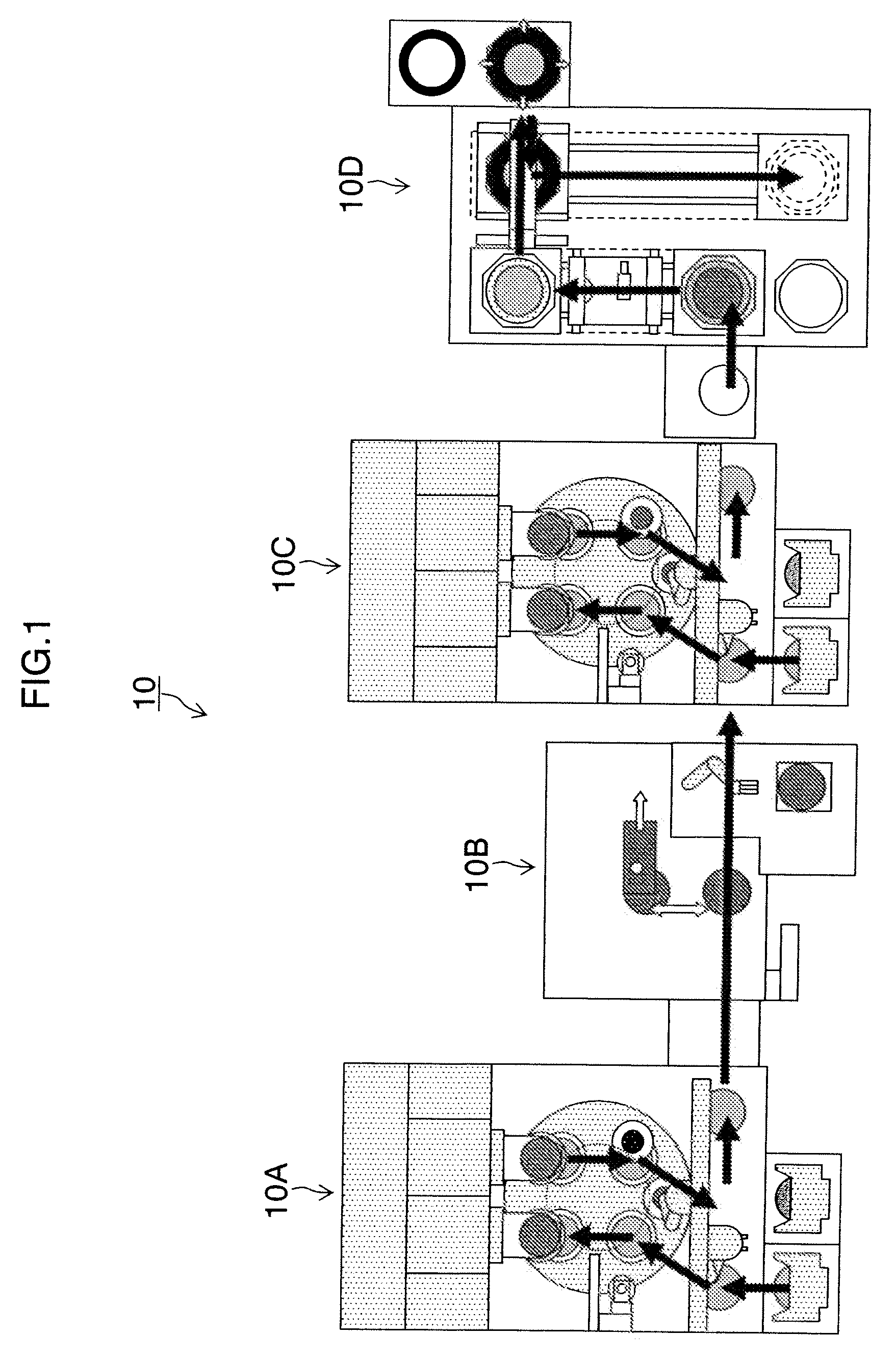
[0052]FIG. 1 is a plan view showing an overall configuration of a wafer working system 10 to which the present invention is applied. The wafer working system 10 comprises, from the upstream side (i.e., left-hand side), a surface machining apparatus 10A, a laser dicing apparatus 10B, a surface machining apparatus 10C, and a wafer mounting apparatus 10D. Description will be made of these apparatuses sequentially.

[0053]The surface machining apparatus 10A is used in a first machining step, and the surface machining apparatus 10C is used in a second machining step.

[0054]It is possible to use one surface machining apparatus 10A (or 10C) in both of the first and second machining steps without the provision of two such surface machining apparatuses as shown in FIG. 1.

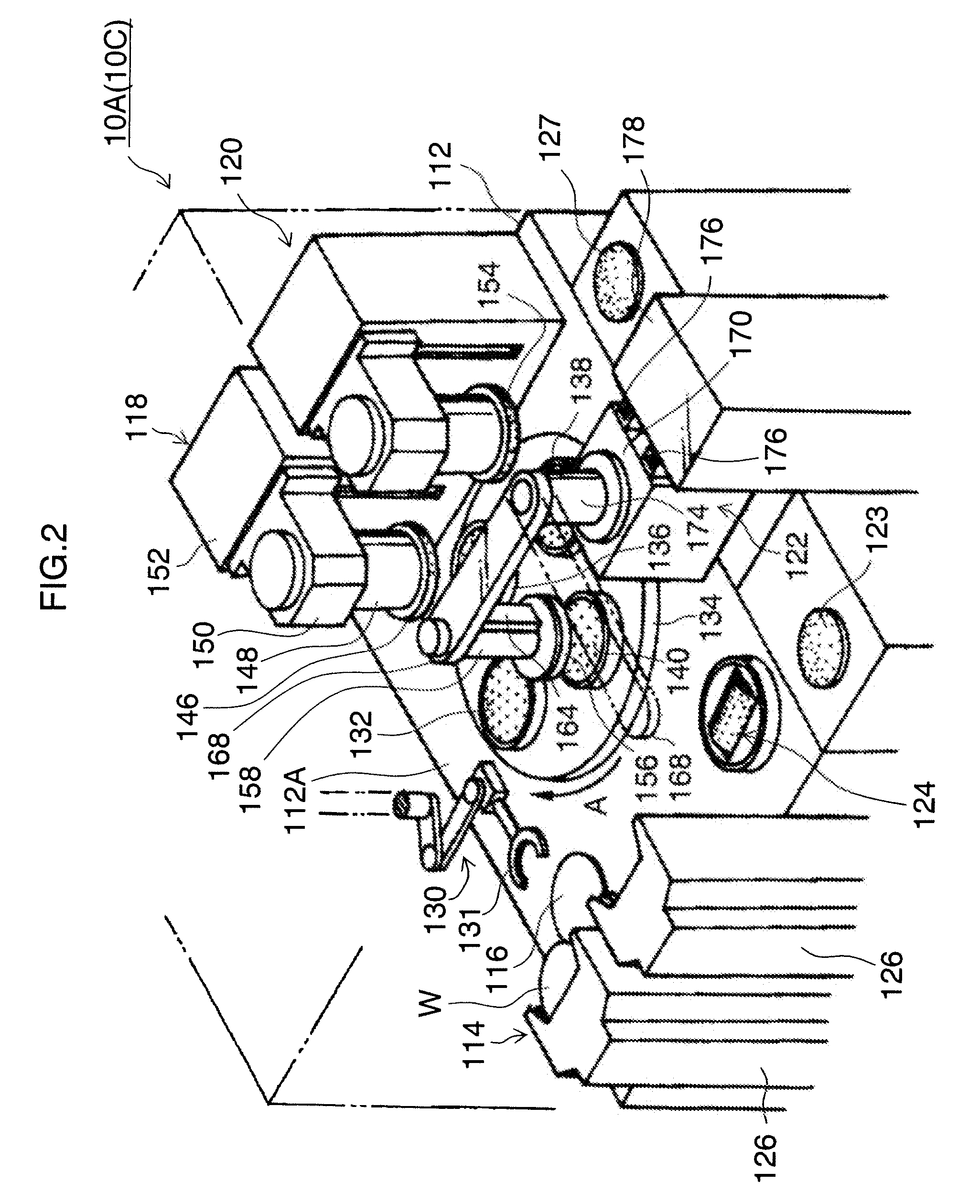
[0055]FIG. 2 is a perspective view of the surface machini...


PUM

PropertyMeasurementUnit
thicknessaaaaaaaaaa
thickness T1aaaaaaaaaa

Abstract

A wafer working method is provided which is capable of feeding a wafer diced by a laser dicing apparatus to a subsequent step without breaking up the wafer. The wafer working method comprises: a first machining step of grinding a reverse side of a wafer W and then polishing the reverse side of the wafer thus ground to a thickness T2 which is larger than a finally worked wafer thickness T1; a modified region forming step of irradiating laser light to a region of the wafer thus subjected to the first machining which lies inwardly of a modification-free zone measuring 0.1 mm to 10 mm from a periphery of the wafer, to form a modified region inside the wafer; and a second machining step of grinding the reverse side of the wafer thus formed with the modified region and then polishing the reverse side of the wafer thus ground to the finally worked wafer thickness T1.

Description

BACKGROUND OF THE INVENTION[0001]1. Field of Invention[0002]The present invention relates to wafer working methods and, more particularly, to a wafer working method suitable for performing a process from surface machining to mounting of a semiconductor wafer cut to a chip size without causing any defect.[0003]2. Description of Related Art[0004]In a process for fabricating a semiconductor device, an electronic component, or the like, it is a general practice to subject a wafer formed with a semiconductor device, an electronic component, or the like on an obverse side thereof to process steps including probing, dicing, die bonding, and wire bonding and then to packaging with resin molding seal, to give a finished product of the semiconductor device, electronic component, or the like.[0005]In recent years, there has been increasing demand for a very thin semiconductor device or electronic component to be incorporated into a memory card, a thin IC card, or the like. Accordingly, increas...

Claims


Application Information

Patent Timeline
Patent Type & Authority Applications(United States)
IPC IPC(8): H01L21/00C25F3/00B23K26/38
CPCB23K26/0853B23K26/0876B23K26/4075B23K2201/40B24B37/04H01L21/3043B23K26/0057H01L21/67115H01L21/67132H01L21/67219H01L21/68764H01L21/68771H01L21/78H01L21/67092B23K26/40B23K26/53B23K2101/40B23K2103/50H01L21/304
Inventor KANEKO, TAKAYUKI
Owner TOKYO SEIMITSU
Why Eureka
Try Eureka