Method and system for optical characterization of optical crystallization

Inactive Publication Date: 2009-01-01
COHERENT GMBH
View PDF0 Cites 0 Cited by
  • Summary
  • Abstract
  • Description
  • Claims
  • Application Information

AI Technical Summary

Benefits of technology

[0009]Methods and systems in accordance with the present invention enable accurate and reliable inspection of recrystallization processes. The invention is generally based upon optical control methods.
[0010]One aspect of the invention relates to a method for characterization of a crystallization process with optical methods, in which a processed substrate is illuminated with polychromatic light. An image of the illuminated substrate is recorded using an image acquisition system that is capable of acquiring color images. The recorded image is then transmitted to an image processing unit that analyzes the image color selectively. This enables faster scans and more reliable results than analyzing color images with conventional methods. The image processing unit analyzes the green and / or the blue channel of the recorded image separately. It has been found that different stages of recrystallization show different optical properties, especially in the green and blue channel of a color image. The red channel exhibits only very small contrasts. Limiting the analysis to the green and / or blue channel saves calculation resources and improves the contrast between the different phases. It is particularly advantageous to further optimize the contrast of the blue and / or the green channel of the image. The regions of interest, particularly the borders between crystallized areas and amorphous areas and uncrystallized spots in the areas to be crystallized, are more visible after contrast optimization.
[0011]Another aspect of the invention relates to a method for characterization of a crystallization process with optical methods in which a crystallizing substrate is illuminated with a substantially monochromatic light or a narrow band polychromatic light. An image of the substrate is recorded using an image acquisition system and the recorded image is transmitted to an image processing unit. The image processing unit analyzes the recorded image. This aspect of the invention enables the use of black and white cameras that usually have a higher resolution than color cameras, since color cameras usually use three sensor elements for one pixel of an image. Furthermore, black and white cameras are cheaper than color cameras because the image sensor technology is less complex.
[0012]It is particularly advantageous to use light emitting diodes for illumination. Diodes which irradiate blue and green light have shown best results. The use of color light diodes enables faster switching between different illumination colors than the use of, for example, different color filter elements in front of white light or broad band illumination systems.

Problems solved by technology

These requirements place great demands on the process control of SLS system.
One drawback of this conventional method is that it is difficult to automate; the images usually must be inspected by a qualified person.
There are a number of challenges associated with an optical approach to recrystallization control.
First, the inspected structures of recrystallization are rather small.

Method used


Image

  • Method and system for optical characterization of optical crystallization
  • Method and system for optical characterization of optical crystallization
  • Method and system for optical characterization of optical crystallization

Examples


Embodiment Construction

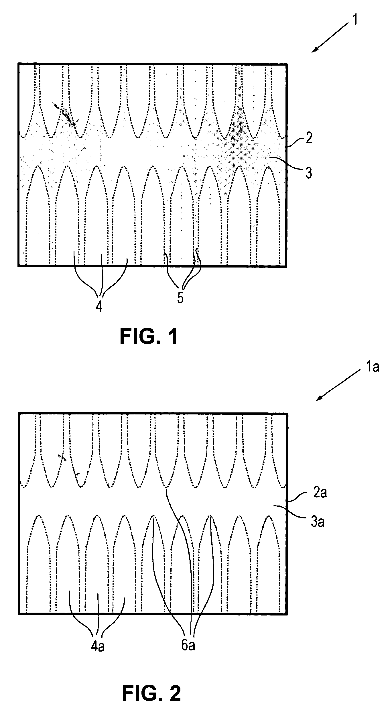
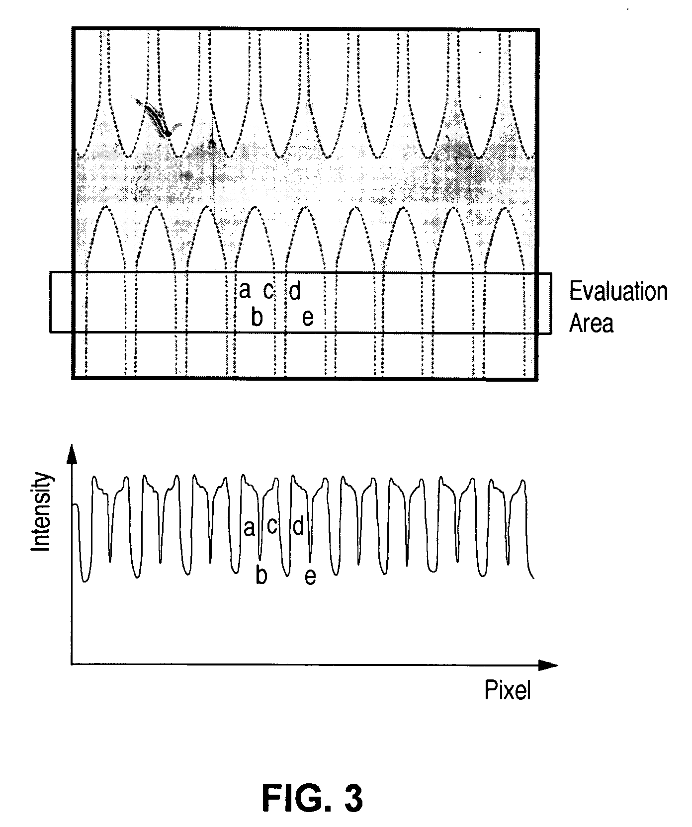
[0024]FIG. 1 shows an image 1 of a partially sequential lateral solidification (SLS) treated silicon substrate 2 which has been acquired utilizing a color camera. The substrate 2 exhibits amorphous silicon in area 3 of the substrate 2. The substrate 2 further shows recrystallized substrate (all of what is not area 3) protrusion lines 4 and borders of the recrystallized substrate in which the substrate has been treated by an SLS process in a known way.

[0025]For quality purposes, it is important that the profile of the recrystallized substrate remains homogeneous over the full substrate area. That is, position and width of the protrusion lines 4 and the borders 5 should not change. Inhomogenities will lead to visible deviations of cell performance, e.g., in TFT displays, and, therefore, are not desirable. (The black bent line in the top left part of FIGS. 1-5 is a dust particle.)

[0026]FIG. 2 shows the red channel of the color image 1 of FIG. 1. The red channel of the image 1a contains...


PUM


Abstract

Systems and methods for optical characterization of crystallization processes, especially SLS crystallization processes, are disclosed. A substrate is illuminated with light and images are acquired by image acquisition means. The images of the processed areas are fed to a control system. The control system works color selectively by either using color selective image processing of color images or by the use of colored light and black and white image acquisition means.

Description

FIELD OF THE INVENTION[0001]The present invention relates to techniques for controlling crystallization processes and, in particular, to methods and systems for optical control of sequential lateral solidification (SLS) crystallization processes.BACKGROUND OF THE INVENTION[0002]Thin film transistor (TFT) technology is the basis for high-resolution, high-performance liquid crystal display (LCD) screens, providing the best resolution of the various flat panel display technologies that are currently available. Advanced thin film transistor technology is based upon polycrystalline silicon.[0003]Polycrystalline silicon may be formed using laser recrystallization techniques, such as excimer laser annealing. In excimer laser annealing, a high-power laser beam is scanned over the surface of a substrate that is coated with amorphous silicon. The amorphous silicon is heated, melts and then recrystallizes to form polycrystalline silicon.[0004]A more recently introduced laser recrystallization ...

Claims


Application Information

Patent Timeline
IPC IPC(8): H04N5/00
CPCG06T7/0004H01L21/2026G06T2207/30108H01L21/02686H01L21/02691H01L21/02532H01L21/02678H01L21/02667
Inventor WENZEL, THOMASSIMON, FRANK
Owner COHERENT GMBH
Why Eureka
Try Eureka