
Capacitive input device

Active Publication Date: 2008-12-18
JAPAN DISPLAY WEST
View PDF6 Cites 472 Cited by
  • Summary
  • Abstract
  • Description
  • Claims
  • Application Information

AI Technical Summary

Benefits of technology

[0011]An advantage of an aspect of the invention is to provide a capacitive input device which can be manufactured by a simple process and in which electrode lines on a translucent substrate and intersecting portions between the electrode lines are inconspicuous.
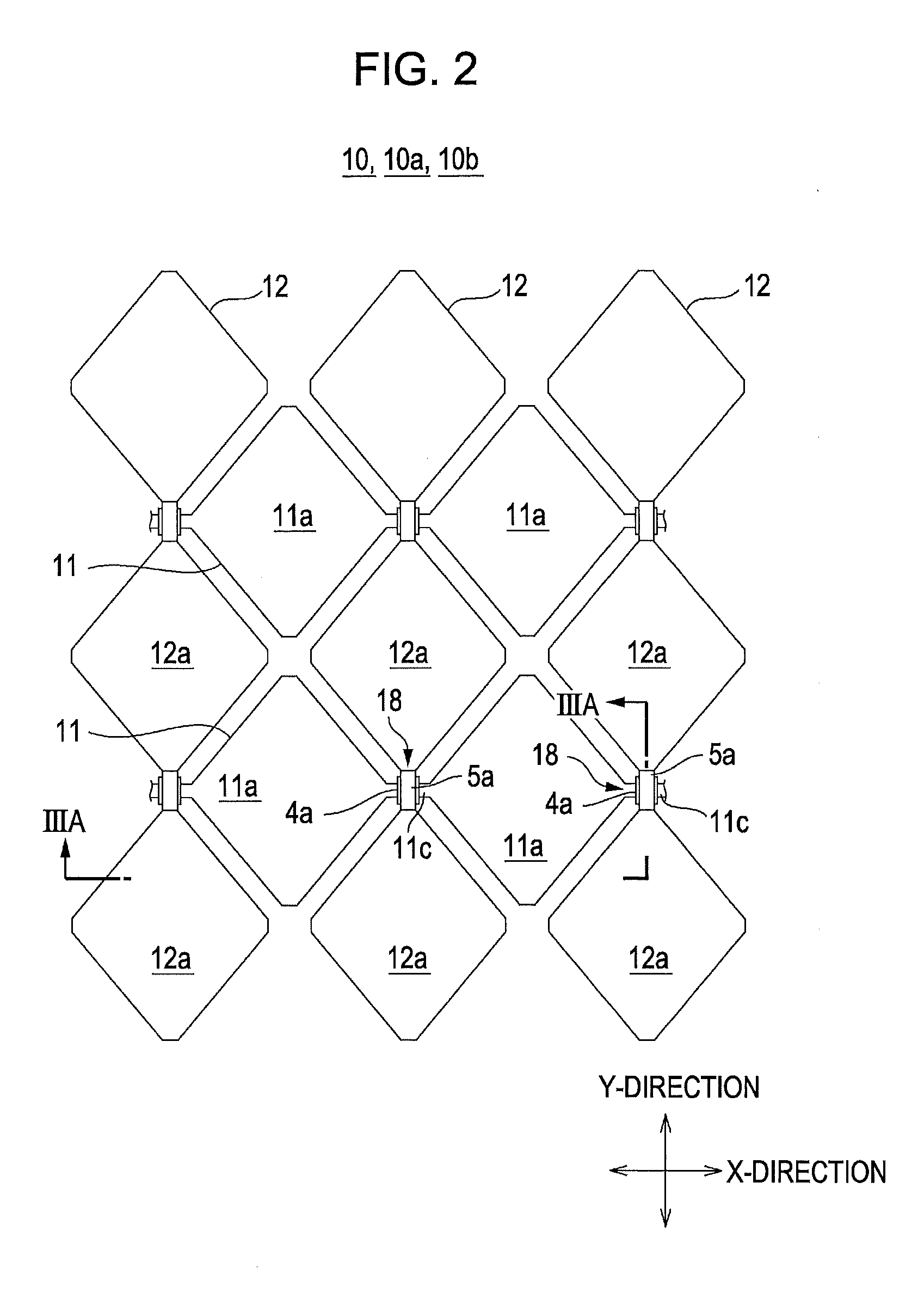
[0014]In the capacitive input device, the first and second translucent electrode lines are preferably formed from the same member. Therefore, the capacitive input device can be manufactured by a simpler process as compared to capacitive input devices including first and second translucent electrode lines formed from different members.
[0016]In the capacitive input device, the first and second translucent electrode lines are preferably formed from a multilayer film including translucent thin-films having different refractive indexes. This leads to a reduction in the difference in reflectivity between the region containing the first and second translucent electrode lines and the region containing no first and second translucent electrode lines; hence, the first and second translucent electrode lines are inconspicuous when the capacitive input device is viewed from the input screen side. In general, the light traveling from a medium with a small refractive index to a medium with a large refractive index is reflected by the interface between the media. Since the first and second translucent electrode lines are arranged on the translucent substrate, the following interfaces are present: the interface between each first or second translucent electrode line and an air layer located on the input screen side and the interface between the translucent substrate and the first or second translucent electrode line; hence, there is a difference in reflectivity between the region containing the first and second translucent electrode lines and the region containing no first and second translucent electrode lines. This may cause the first and second translucent electrode lines to be conspicuous. The difference in reflectivity between the region containing the first and second translucent electrode lines and the region containing no first and second translucent electrode lines can be eliminated in such a manner that the phases of portions of the light reflected by the interfaces are set to be opposite to each other. This allows the first and second translucent electrode lines to be inconspicuous.
[0020]The capacitive input device may further include a plurality of metal wires which are connected to the first and second translucent electrode lines and which extend outside the input region. This leads to a reduction in wiring resistance.

Problems solved by technology

Therefore, the resistive touch panels have disadvantages that they have a narrow operational temperature range and deteriorate with time.
There is a problem in that a process for manufacturing the following device is complicated: a capacitive input device that includes a translucent substrate, a plurality of first translucent electrode lines which extend in a first direction and which are disposed on the front surface of the translucent substrate, and a plurality of second translucent electrode lines which extend in a second direction intersecting with the first direction and which are disposed on the rear surface of the translucent substrate.
This results in large differences in reflectivity between these regions to cause a problem that the first and second translucent electrode lines are conspicuous.

Method used


Image

  • Capacitive input device
  • Capacitive input device
  • Capacitive input device

Examples


first embodiment

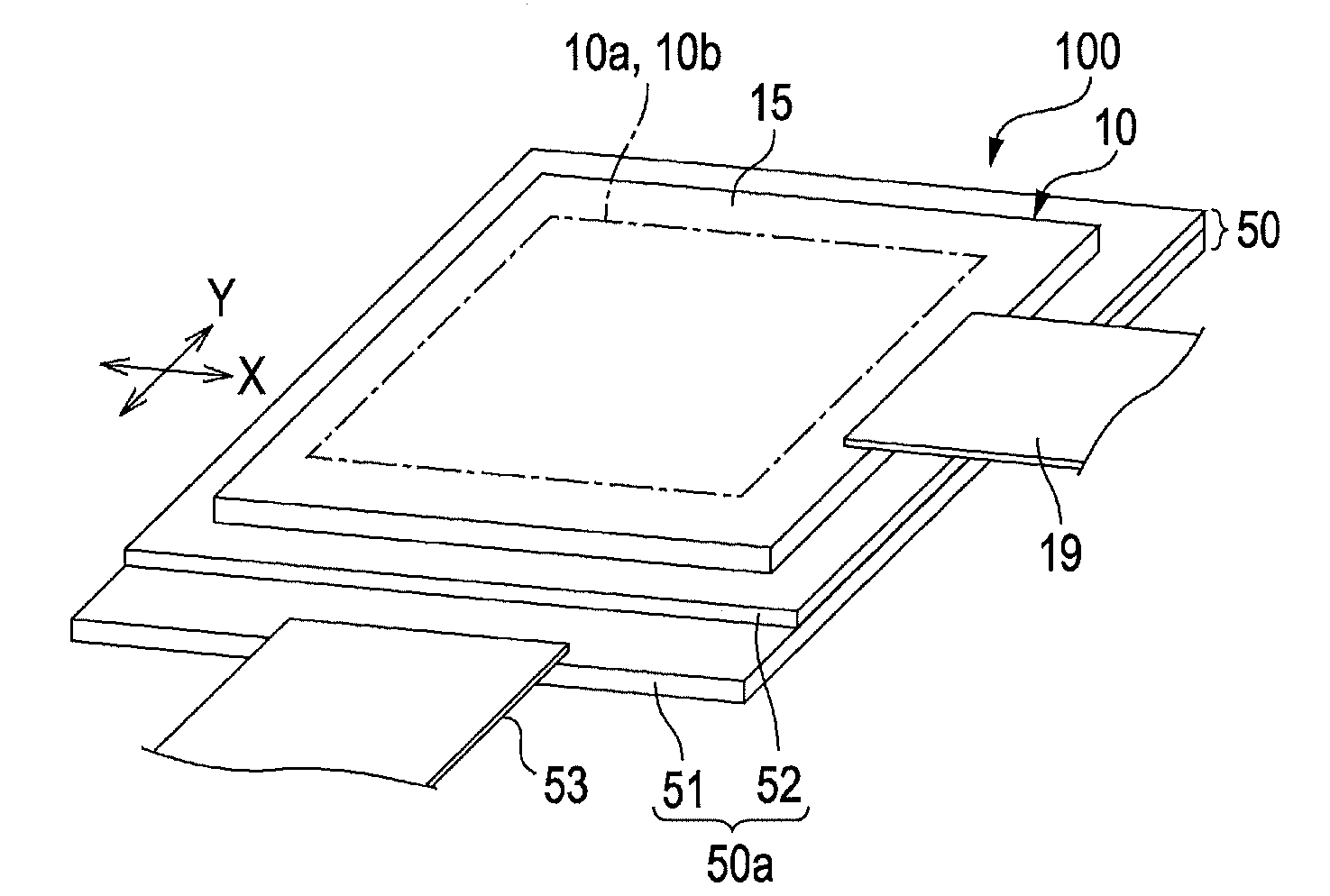
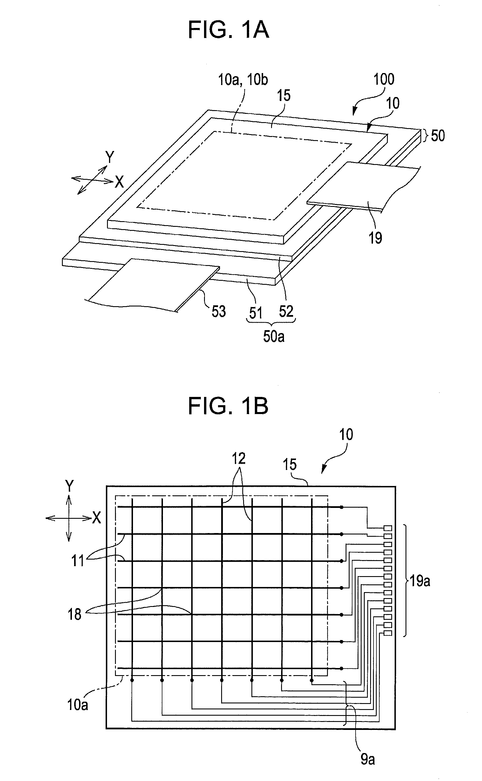
[0037]FIG. 1A is schematic view of a display unit 100. FIG. 1B is a plan view of the display unit 100. With reference to FIG. 1B, solid lines simply represent electrode lines, of which the number is less than that of actual electrode lines.

[0038]With reference to FIG. 1A, the display unit 100 includes a panel-shaped capacitive input device 10 according to a first embodiment of the present invention and a liquid crystal display 50 functioning as an image generator. The liquid crystal display 50 has a first surface through which light is emitted. The capacitive input device 10 is disposed on the first surface of the liquid crystal display 50. The liquid crystal display 50 includes an active matrix-type liquid crystal display panel 50a that is transmissive, reflective, or transflective. When the liquid crystal display panel 50a is transmissive or transflective, a backlight (not shown) is placed on the side opposite to the first surface. The liquid crystal display 50 further includes a ...

second embodiment

[0063]FIG. 5 is a plan view showing the arrangement of first translucent electrode lines 11 and second translucent electrode lines 12 included in a capacitive input device 10 according to a second embodiment of the present invention. FIG. 6A is a sectional view of the capacitive input device 10 taken along the line VIA-VIA of FIG. 5. FIG. 6B is a sectional view showing connections between the first and second translucent electrode lines 11 and 12 and metal wires 9a. A configuration described in this embodiment is similar to that described in the first embodiment. Therefore, components common to the first and second embodiments have the same reference numerals and will not be described in detail.

[0064]The capacitive input device 10, as well as that of the first embodiment, is a type of touch panel. With reference to FIGS. 5 and 6A, the capacitive input device 10 includes a translucent substrate 15, made of glass, including an input screen 10b having an input region 10a. The first and...

third embodiment

[0080]Examples of an electronic apparatus including a display unit 100 including the capacitive input device 10 according to the first or second embodiment will now be described. FIG. 8A shows a mobile personal computer 2000. The personal computer 2000 includes the display unit 100 and a body 2010. The body 2010 includes a power switch 2001 and a keyboard 2002. FIG. 8B shows a mobile phone 3000. The mobile phone 3000 includes the display unit 100, a plurality of operation buttons 3001, and a plurality of scroll buttons 3002. The operation of the scroll buttons 3002 allows an image displayed on the display unit 100 to be scrolled. FIG. 8C shows a personal digital assistant (PDA) 4000. The PDA 400 includes the display unit 100, a plurality of operation buttons 4001, and a power switch 4002. The operation of the power switch 4002 allows various pieces of information, such as addresses and schedule tables, to be displayed on the display unit 100.

[0081]Examples of the electronic apparatu...


PUM


Abstract

A capacitive input device includes a translucent substrate; first translucent electrode lines, extending in a first direction; second translucent electrode lines, extending in a second direction intersecting with the first direction; interlayer insulating layers; and relay electrodes. The first translucent electrode lines intersect with the second translucent electrode lines at intersecting portions. Portions of one of each first translucent electrode line and each second translucent electrode line are connected to each other with the intersecting portions. Portions of the other are separated from each other with the intersecting portions. The translucent interlayer insulating layers overlie the first or second translucent electrode line portions connected to each other with the intersecting portions. The translucent relay electrodes overlie the interlayer insulating layers to electrically connect the first or second translucent electrode line portions, separated from each other with the intersecting portions, to each other.

Description

[0001]The entire disclosure of Japanese Patent Application No. 2007-157115, filed Jun. 14, 2007 is expressly incorporated by reference herein.BACKGROUND[0002]1. Technical Field[0003]The present invention relates to a capacitive input device capable of detecting a position touched by a human finger as a change in capacitance.[0004]2. Related Art[0005]Recent electronic apparatuses such as mobile phones, car navigation systems, personal computers, ticket-vending machines, and banking terminals include tablet input devices disposed on liquid crystal displays. With reference to instruction images displayed on image display regions of the liquid crystal displays, information relating to the instruction images can be input into the electronic apparatuses by the touch of human fingers to the image display regions.[0006]Examples of such input devices include resistive touch panels and capacitive touch panels. The resistive touch panels have a two-layer structure including a glass sheet and a...

Claims


Application Information

Patent Timeline
IPC IPC(8): G06F3/041
CPCG06F3/044G06F2203/04103G06F2203/04111G06F3/0443G06F3/0446G06F2203/04804G06F3/0445
Inventor MATSUO, MUTSUMI
Owner JAPAN DISPLAY WEST
Learn More