
Method and structure for domino read bit line and set reset latch

Inactive Publication Date: 2008-12-04
IBM CORP
View PDF3 Cites 14 Cited by
  • Summary
  • Abstract
  • Description
  • Claims
  • Application Information

AI Technical Summary

Benefits of technology

[0009]It is therefore an object of the invention to provide a bit line structure for a small SRAM array with thirty-two word lines or less which requires less devices and which in turn has a reduced power consumption without losing array access performance.
[0013]According to a preferred embodiment of the invention, during write operations, input latch signals are brought directly to local bit line write circuitry, in order to eliminate the need for global write bit lines. Removing the global write bit lines reduces the total number of NFETs in series required to pull down the local bit line to ground during a write operation from three to two which improves the write performance and write margin of the SRAM cell significantly.
[0014]Compared to the prior art bit line structure, the structure claimed herein reduces the number of devices significantly, which saves area and reduces AC and DC power consumption. The bit line structure according to preferred embodiments realized with significantly fewer transistors than prior art implementations, which reduces the layout area by approximately 35%. A lower device count reduces the DC (direct current) leakage power. The preferred embodiments also dissipate 50% less AC (alternating current) power because there are fewer nets switching every cycle (no global read or write bit lines). Also, the output of the set-reset latch is single-ended and switches only when the input data is different than the current latch state so all downstream logic switches only when necessary. The read access time is reduced by approximately 5% by eliminating two stages of logic. Similarly, the write time is improved because there are only two NFETs in series to pull down the local bit line and because the input data signals are shorter in length.
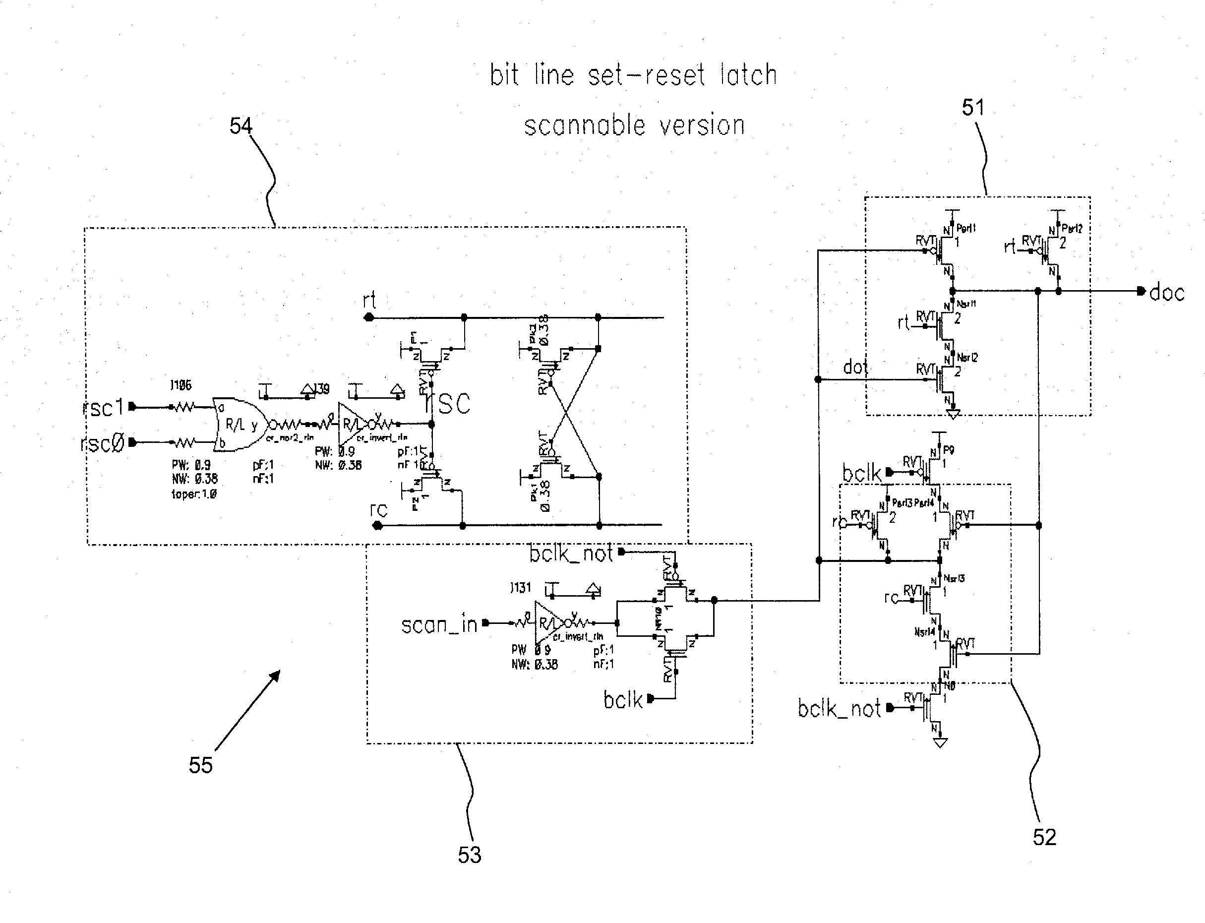
[0016]A shift port and gating element are used to propagate the true and complement outputs serially through the set-reset latch. The NAND elements are gated by a shift clock during a test operation. The shift clock avoids the dissipation of active feedback current through the NAND gate This allows a more efficient operation for the set reset latch because the active feedback current is switched off during the time the shift port is open for overwriting the latch content. This circuit topology allows an increased robustness for operations at minimum voltage compared to a solution without gating one of the NANDs. This is because the two NANDs together form a feedback loop that without gating one NAND could only be overwritten when the circuits are operating in a higher voltage range. The shift port preferably uses a shift input and at least one shift clock input which are active during test operations.

Problems solved by technology

The global bit lines and the support circuitry are a significant percentage of the small array's area and power consumption.
Because the global bit lines are implemented both true and complement lines, one or the other of these global bit lines are always being reset every cycle, which consumes AC power.

Method used


Image

  • Method and structure for domino read bit line and set reset latch
  • Method and structure for domino read bit line and set reset latch
  • Method and structure for domino read bit line and set reset latch

Examples


Embodiment Construction

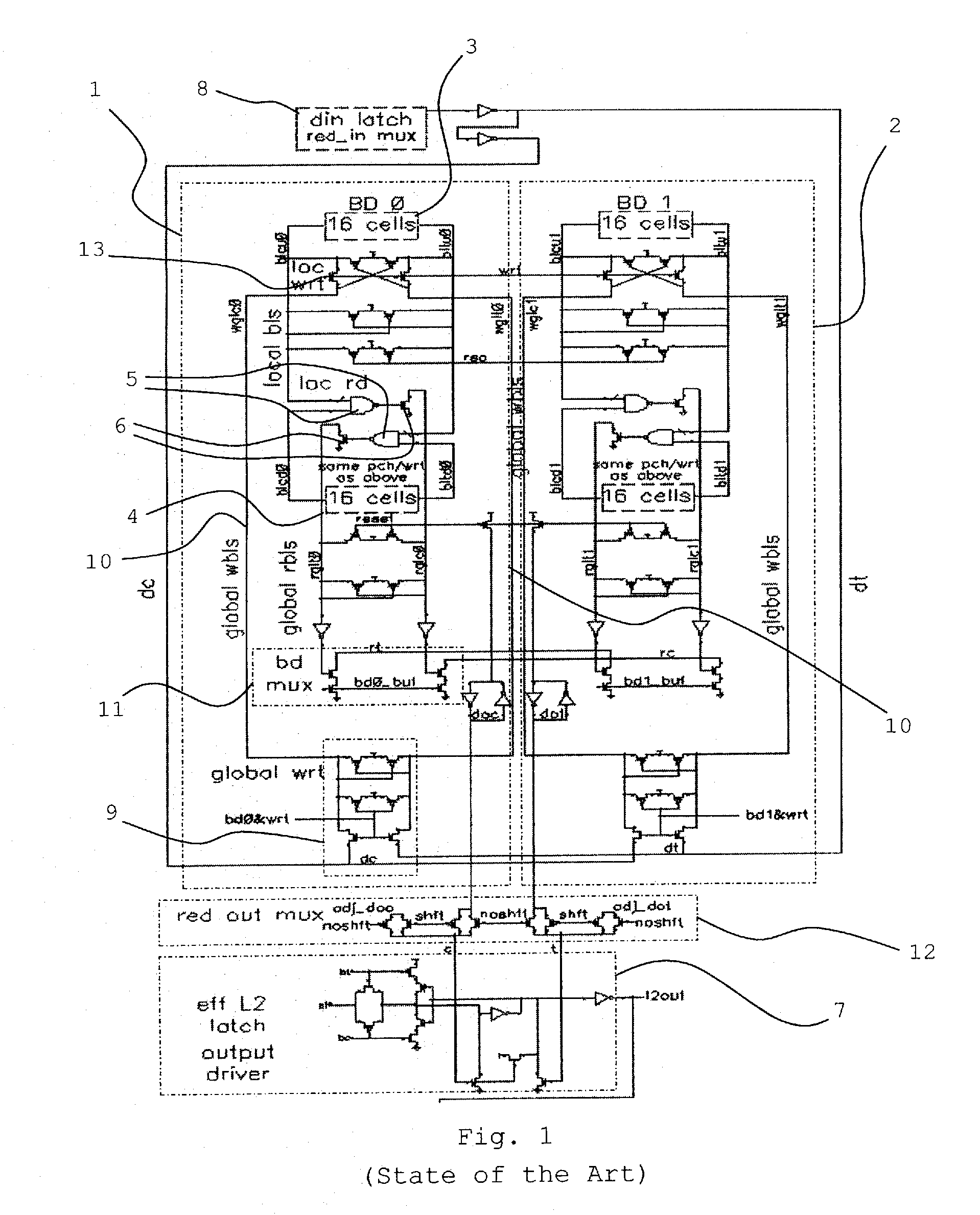
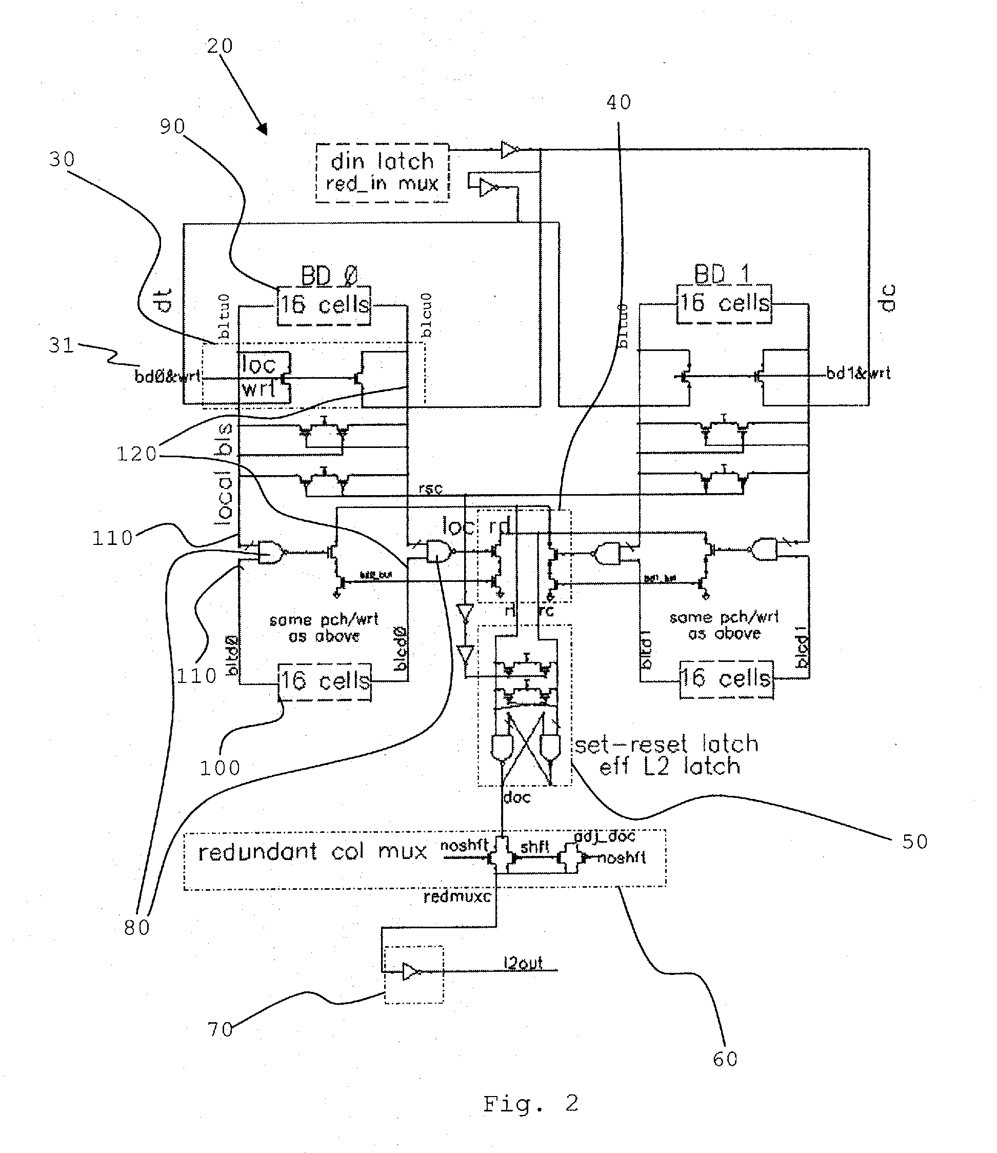
[0022]A bit line structure 20 according to a preferred embodiment is shown in FIG. 2, which achieves a significant reduction in device count as compared to the prior art implementation of FIG. 1. This device reduction is achieved by completely removing the read global bit line structures (rglt0 and rglc0 in FIG. 1) and write global bit line structures (wglc0 and wglt0 in FIG. 1). This is made possible by combining the bit decode multiplexer (11 in FIG. 1) directly into the local evaluation circuitry (80 and 40 in FIG. 2) and by incorporating the column select signal (bd0&wrt in FIG. 1) into the local write control signal of FIG. 2.

[0023]The true and complement local bit lines bltu0 and blcu0 from the upper 3, and bltd0 and blcd0 from the lower group 4 (FIG. 1) and 110 and 120 respectively (FIG. 2) are read in the same manner in both approaches. They are pre-charged high and realize the same capacitive load. This guarantees the same read margin for the array as in the bit line struct...


PUM


Abstract

A domino read bit line structure (20) integral to an SRAM array (1, 2) with thirty-two word lines or less to access SRAM cells divided into two groups (3, 4, 90, 100) is described. The bit line structure (20) includes a dynamic bit decode multiplexer (11, 40) and two NAND circuits (5, 80) used to combine the two groups (3, 4, 90, 100), wherein in order to reduce power consumption the two NANDS (80) drive the dynamic bit decode multiplexer (40) directly, such that true and complement dynamic outputs (rt, rc) drive a set-reset latch (50) to convert the dynamic outputs (rt, rc) to a single static signal (doc), wherein the output of the set-reset latch (50) is already static so that the set-reset latch (50) acts as an effective array output latch (7).

Description

CROSS REFERENCES TO RELATED APPLICATION[0001]This application is related to one European Application No. 07104632.0 filed Mar. 22, 2007FIELD OF THE INVENTION[0002]The invention relates to a domino read bit line structure in conjunction with a small static random access memory (SRAM) array with thirty-two word lines or less plus a set-reset latch for such a bit line structure, which allows to evaluation of the SRAM array during test.BACKGROUND OF THE INVENTION[0003]SRAM is a type of semiconductor memory in which the memory retains its contents as long as power remains applied, unlike dynamic random access memory (DRAM) which needs to be periodically refreshed. Each bit in an SRAM is stored in a storage cell comprising four transistors that form two cross-coupled inverters. This storage cell has two stable states which are used to denote ‘0’ and ‘1’. Two additional access transistors serve to control the access to a storage cell during read and write operations. It thus typically take...

Claims


Application Information

Patent Timeline
IPC IPC(8): G11C7/00G11C8/00
CPCG11C11/41G11C29/12G11C2029/1204
Inventor CHAN, YUEN HUNGHOULE, ROBERT MAURICESAUTTER, ROLFWITTE, PASCAL
Owner IBM CORP
Learn More