
Image sensor

a technology of image sensor and image, which is applied in the field of image sensor, can solve the problems of limited use of ccds in the market, current leakage (that, dark current) problem, etc., and achieve the effect of improving dark current and good light shielding properties

Active Publication Date: 2008-10-30
UNITED MICROELECTRONICS CORP +1
View PDF17 Cites 16 Cited by
  • Summary
  • Abstract
  • Description
  • Claims
  • Application Information

AI Technical Summary

Benefits of technology

[0012]An object of the present invention is to provide a manufacturing method of an image sensor device to manufacture an image sensor device having an improved dark current, as well as excellent light shielding properties in the optical black region.
[0013]Another object of the present invention is to provide an image sensor device having a relatively low dark current while still having good light shielding properties in the optical black region.
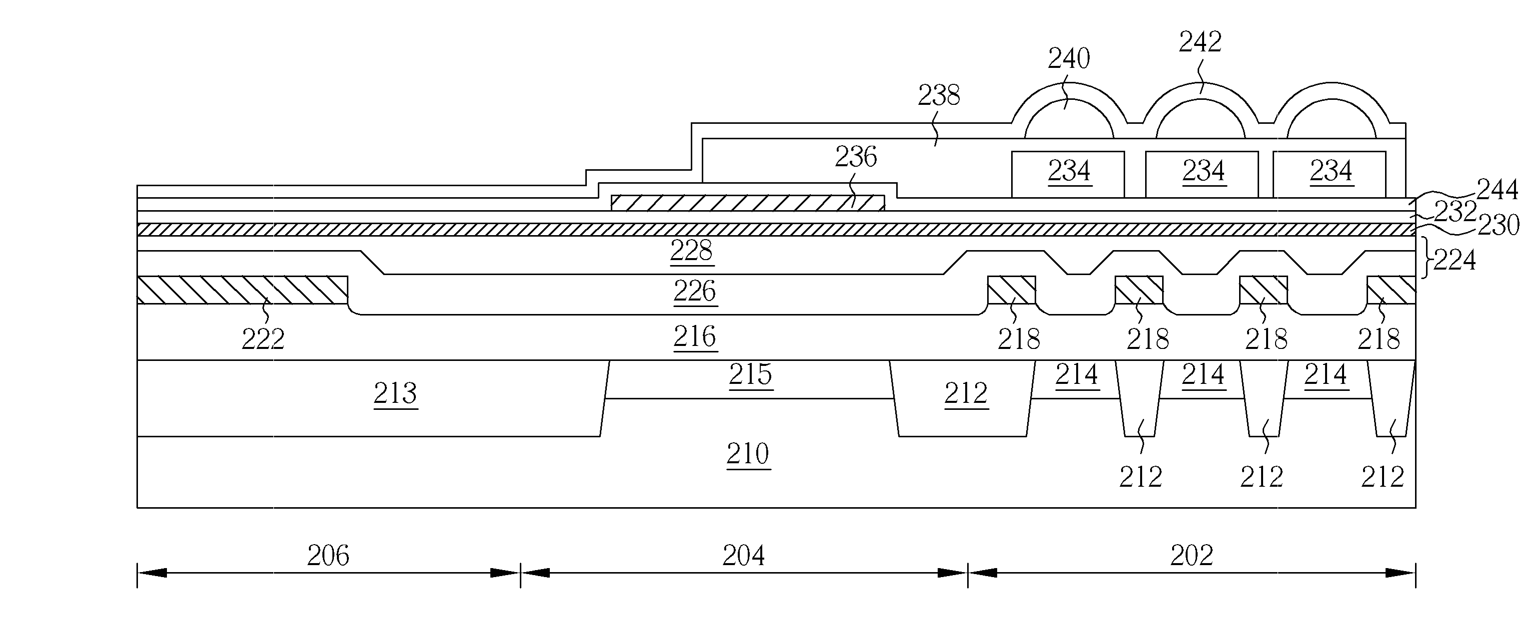
[0016]In the method of manufacturing an image sensor device according to the present invention, a light-shielding metal layer as conventionally used in the optical black region is not formed, and instead, an optical black layer comprising metal having has good light shielding properties is formed after a passivation layer is formed and before a color filter array is formed. Therefore, in the dangling bond passivation process by annealing, the passivation of the dangling bonds in the optical black region is more efficient without impedance by a conventional light shielding metal layer. Thereafter, an optical black layer can be formed from a material comprising metal at a relatively low temperature, and an image sensor device having an improved dark current can be obtained.

Problems solved by technology

CCDs use is limited in the market due to price and the volume considerations.
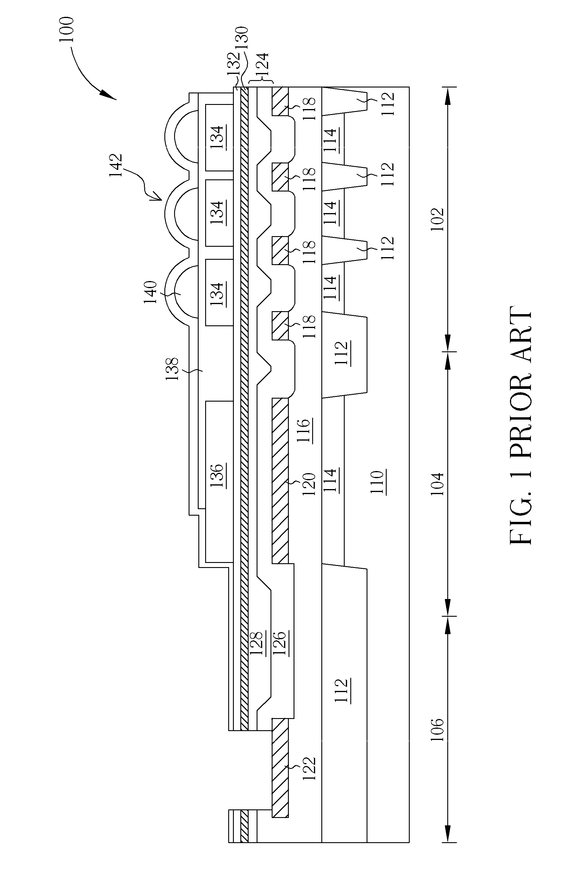
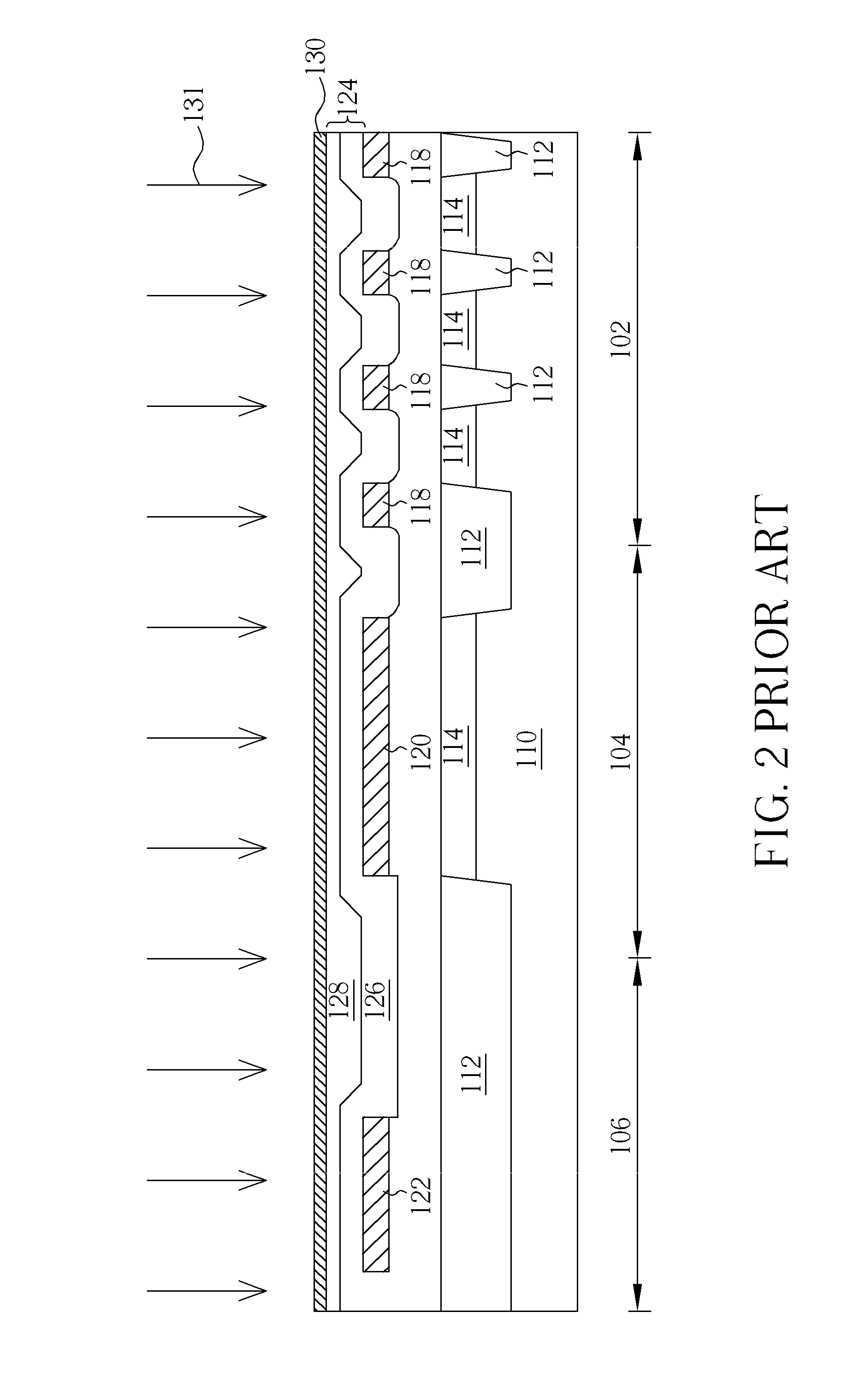
However, during the manufacturing process of a conventional CMOS image sensor, after the passivation layer 130 is formed, the photodiodes often have plenty of dangling bonds on the surface, leading to a current leakage (that is, dark current) problem.
However, a patterned metal layer 120 for light shielding contains metal atoms which may react with the hydrogen, and as a result, the removal of dangling bonds is impeded by the metal layer 120.

Method used


Image

  • Image sensor
  • Image sensor
  • Image sensor

Examples


Embodiment Construction

[0023]Please refer to FIG. 3 showing an image sensor device 200 according to the present invention. The image sensor device 200 comprises a semiconductor substrate 210, a pixel array region 202, a logic region 206, and an optical black region 204. The pixel array region 202 is on the semiconductor substrate 210 and comprises a photo sensing unit array 214. The logic region 206 is on the semiconductor substrate 210 and comprises a peripheral circuit. The optical black region 204 is positioned between the pixel array region 202 and the logic region 206 on the semiconductor substrate and comprises a photo sensing unit 215 on the semiconductor substrate 210, a first planarized layer 216 on the photo sensing unit 215, a second planarized layer 224 on the first planarized layer 216, and a optical black layer 236 on the second planarized layer 224.

[0024]It is noted that the optical black layer 236 comprises a metal layer formed at a low temperature, for example less than 400° C. The metal ...


PUM


Abstract

An image sensor, in which, a planarized layer is formed on a semiconductor substrate including a pixel array region, an optical black region, and a logic region to cover a photo sensing unit array in the pixel array region, a patterned metal layer is formed on the planarized layer corresponding to the pixel array region and the logic region, but not the optical black region. An optical black layer is formed in the optical black region after a passivation layer is formed and before a color filter array is formed at a temperature less than about 400° C., and preferably contains metal material.

Description

CROSS REFERENCE TO RELATED APPLICATIONS[0001]This is a divisional application of U.S. patent application Ser. No. 11 / 461,457 filed on Aug. 1, 2006, and the contents of which are included herein entirely by reference.BACKGROUND OF THE INVENTION[0002]1. Field of the Invention[0003]The present invention relates to an image sensor and a method of manufacturing the same, and more particularly to, a CMOS image sensor and a method of manufacturing the same.[0004]2. Description of the Prior Art[0005]CMOS image sensors (CISs) and charge-coupled devices (CCDs) are optical circuit components for utilization with light signals and representing the light signals as digital signals. CISs and CCDs are used in the prior art. These two components are widely applied to many devices, including scanners, video cameras, and digital still cameras. CCDs use is limited in the market due to price and the volume considerations. As a result, CISs enjoy greater popularity in the market.[0006]Since a CMOS image...

Claims


Application Information

Patent Timeline
Patent Type & Authority Applications(United States)
IPC IPC(8): H01L31/0232
CPCH01L27/14623H01L27/14627H01L27/14634H01L27/14685H01L27/14687H01L27/14689
Inventor WEN, TZENG-FEIROSSI, GIUSEPPEYEN, JU-HSINLIN, CHIA-HUEISZE, JHY-JYIHUANG, CHIEN-YAOKO, TENG-YUANPENG, NIEN-TSU
Owner UNITED MICROELECTRONICS CORP
Learn More