


Quick Research
Generate reliable direction feasibility study reports for your R&D in just a few steps.

Technical Q&A
Discover and master advanced knowledge NOW. Basics, ideas, possibilities, all at once.

Find Solutions
As an expert in R&D theories, this can generate solutions to your technical problems instantly.

Evaluate Feasibility
Analyze your overall solution with one click, know your potential R&D risks in advance.

Monitor Landscape
Get weekly tech updates, stay abreast of the latest tech innovations and key insights.
Flash memory device and fabricating method thereof
a flash memory and fabrication method technology, applied in the field of flash memory devices, can solve the problems of large-scale integration, increase the distribution of threshold voltage, and the scale gate length downscaling of the existing flash memory devices having under 60 nm scale gate length is on the verge of limitation, so as to improve the fast erase characteristic, reduce the threshold voltage shift, and increase the channel controllability of the control electrode.
- Summary
- Abstract
- Description
- Claims
- Application Information
AI Technical Summary
Benefits of technology
Problems solved by technology
Method used
Image

Examples
Embodiment Construction
[0047]Hereinafter, referring to appended drawings, the structures and operational principles for the embodiments of present invention are described in detail.
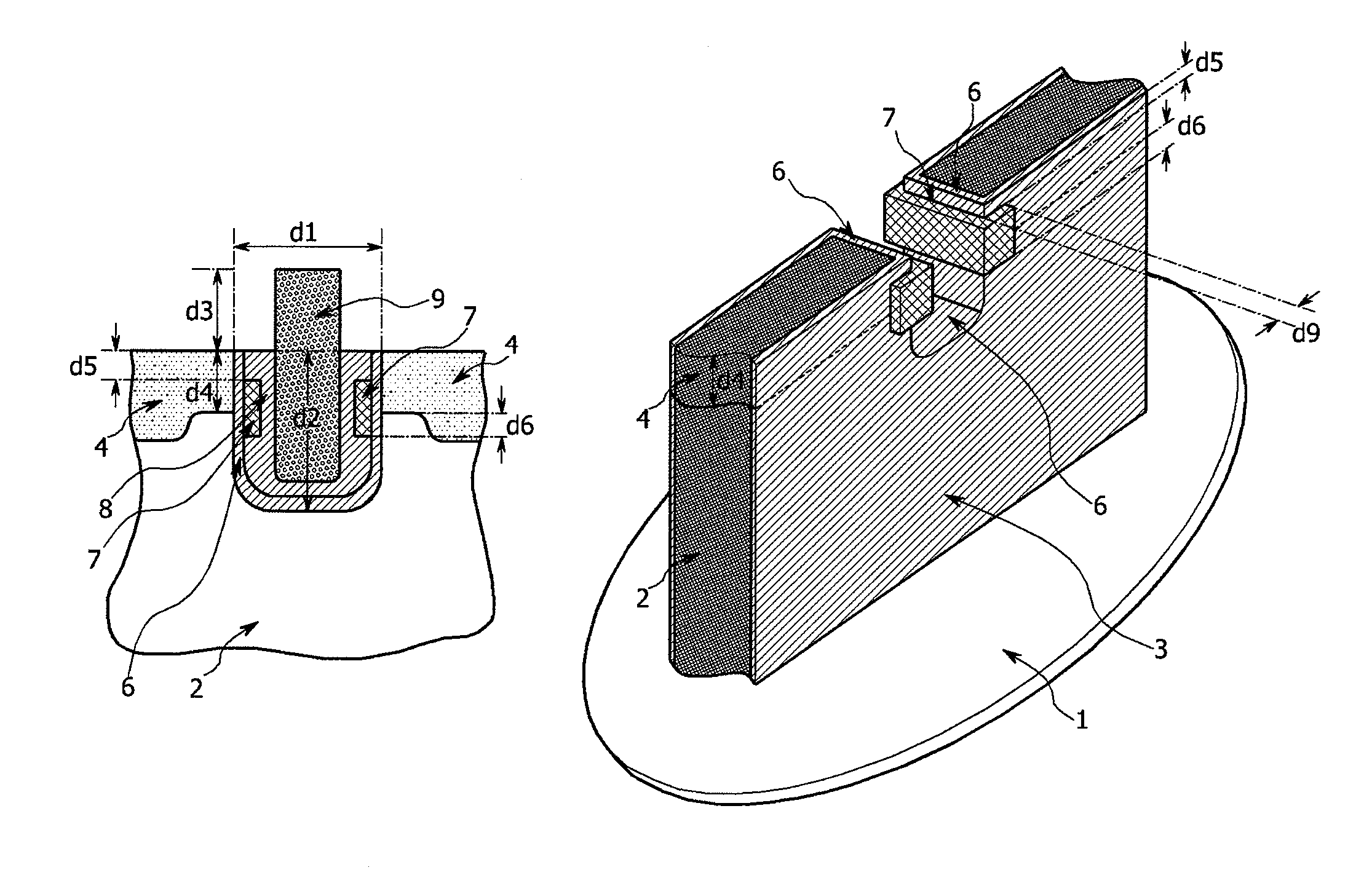
[0048]In the present invention, proposed a novel device structure settling the problems residing in the existing 2-bit / cell structures. FIG. 3(a) shows a cross-sectional view of the device proposed in the present invention, and FIG. 3(b) precisely shows the structure of the present invention, where the process is carried out up to the previous steps which the inter-electrode dielectric film is formed.
[0049]In FIG. 3(b), the field dielectric film region of the truly existing region (5) in order to precisely show a recessed region. And the principal structure around a wall-type body is shown. In FIG. 3(b), the elliptic region (1) indicates a silicon wafer substrate. Basically, the principal parts of a device including storage nodes and channels are made in a recessed region. The width of the wall-type body is suitably formed in a...
PUM
 Abstract
Description
Claims
Application Information
 - R&D Engineer
- R&D Manager
- IP Professional
- Industry Leading Data Capabilities
- Powerful AI technology
- Patent DNA Extraction
Browse by: Latest US Patents, China's latest patents, Technical Efficacy Thesaurus, Application Domain, Technology Topic, Popular Technical Reports.
© 2024 PatSnap. All rights reserved.Legal|Privacy policy|Modern Slavery Act Transparency Statement|Sitemap|About US| Contact US: help@patsnap.com