Image sensor suitable for operating in subresolution mode

a subresolution mode and image sensor technology, applied in the field of image sensors, can solve the problems of insufficient resolution, insufficient energy dissipation, and inability to meet the requirements of pixels, and achieve the effects of reducing pixel sizes, high sensitivity, and increasing power consumption

Inactive Publication Date: 2008-10-02
COMMISSARIAT A LENERGIE ATOMIQUE ET AUX ENERGIES ALTERNATIVES
View PDF8 Cites 1 Cited by
  • Summary
  • Abstract
  • Description
  • Claims
  • Application Information

AI Technical Summary

Benefits of technology

[0011]It is one object of the invention to provide an image sensor for operating in subresolution mode, by therefore averaging the charges generated by several pixels, without requiring the use of numerous additional components, nor increasing the power consumption substantially. A further objective of the invention is to permit operation in subresolution mode, while preserving reduced pixel sizes, and while preserving a high sensitivity, due to an optimal filling factor.
[0020]In another exemplary embodiment, each macro-pixel may comprise a plurality of connecting tracks, connecting the parallel tracks each assigned to a line or a column. In other words, a meshed network is thereby created, serving to reduce the total resistance of the common charge sharing circuit between two diodes.
[0021]In other words, a mesh is thereby obtained around the pixels, in order to place each of the branches of the charge sharing network in parallel. At the same time, the equivalent resistance between the reference voltage source and the reset transistors is reduced.
[0022]In another exemplary embodiment, the various parallel tracks of the common charge sharing circuit in a macro-pixel may be connected to the common connecting track optionally via an additional transistor. In this case, each of the lines or columns assigned to a track may be connected individually to the reference voltage source. This configuration serves to reduce the voltage drop when the photodiodes are recharged, because it limits the length of the track separating each of the pixels with regard to the reference voltage source. In other words, this alternative consists in arranging one connection to the reference voltage source per line.

Problems solved by technology

However, this technique has the drawback of requiring additional components to those of the pixels, that is the capacitance array, which is located outside the pixel matrix.
The presence of this capacitance array therefore increases the volume of the sensor, and above all, causes a dissipation of the energy due to the currents which transit on the column bus bar outside this averaging operation.
However, this solution is not fully satisfactory, insofar as the pixels include several additional transistors, required for connection to the adjacent pixels.
Thus, the larger number of transistors increases the complexity of such a sensor.

Method used


Image

  • Image sensor suitable for operating in subresolution mode
  • Image sensor suitable for operating in subresolution mode
  • Image sensor suitable for operating in subresolution mode

Examples


Embodiment Construction

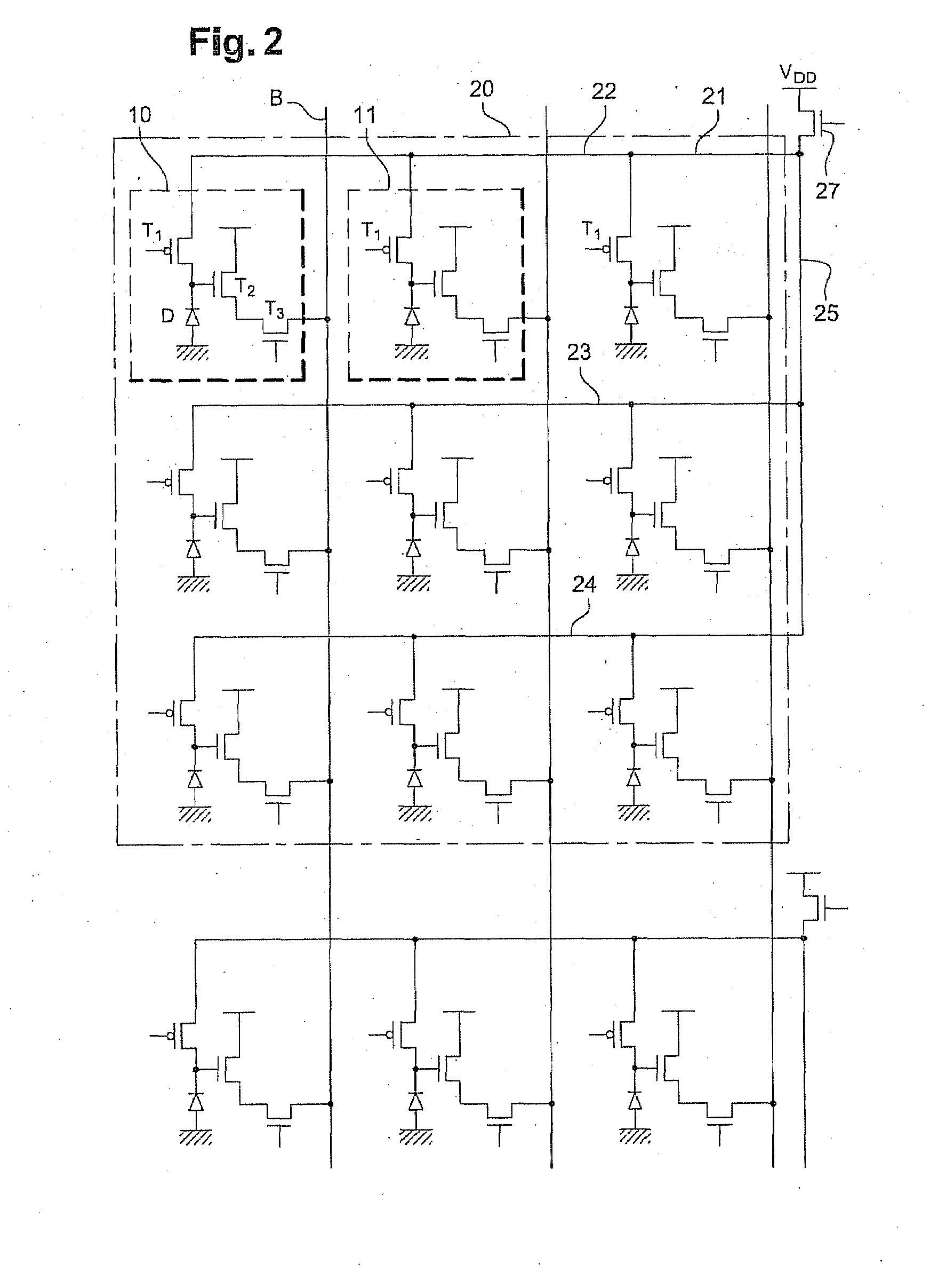
[0030]Conventionally, the image sensor according to the invention comprises, as shown in FIG. 2, a plurality of elementary pixels (10), (11) shown by areas in dotted lines. Each elementary pixel comprises a photodiode (D) whose cathode is connected to the grid of a follower transistor (T2) for converting the photodiode charge into a current. When the selection transistor (T3) is a pass-transistor, this follower transistor delivers to a column bus bar (B1).

[0031]According to the invention, the various elementary pixels are grouped in subsets, in order to define macro-pixels (20), which in the embodiment shown, comprise nine elementary pixels.

[0032]More precisely, each macro-pixel comprises a common electrical connection, a charge sharing network (21). In the embodiment shown in FIG. 2, this network (21) is formed of three tracks (22), (23), (24) parallel to the pixel lines and connected to one end of the connecting track (25) parallel to a column. Thus, each pixel is connected to thi...


PUM


Abstract

“An image sensor suitable for operating in subresolution mode, including a plurality of pixels each formed of an elementary cell including a photodiode, and a reset transistor for connecting the photodiode to a reference voltage source, and a readout transistor connected to a column bus bar for acquiring the value of the charge of the photodiode, where the elementary cells are grouped in subsets forming macro-pixels, each subset having a common electrical connection, to which each elementary cell is able to connect by its reset transistor, in order to share the charges between the photodiodes of the elementary cells of said subset, said common electrical connection being suitable for connection to the reference voltage source.”

Description

FIELD OF THE INVENTION[0001]The invention relates to the field of electronic image sensors and, more precisely, matrix sensors based on CMOS technology. It relates more particularly to a novel architecture of an image sensor, designed for operating in subresolution mode, while preserving high sensitivity.[0002]In fact, operation in subresolution mode serves to produce images corresponding to a smaller volume of data, requiring less computer time for the processing operations, in particular for movement detection operations.PRIOR ART[0003]In general, electronic image sensors comprise an array of elementary cells, arranged in matrix form and each including a photosensitive element whose exposure to light radiation causes the generation of an electric current.[0004]More precisely, and as shown in FIG. 1, each cell (1), in its most simplified version, may comprise three transistors (T1, T2, T3) and a photodiode (D), arranged in an architecture commonly called “3T”. The image is captured...

Claims


Application Information

Patent Timeline
IPC IPC(8): H04N5/335
CPCH04N3/1512H04N3/1562H04N25/709H04N25/76H04N25/77
Inventor VERDANT, ARNAUD
Owner COMMISSARIAT A LENERGIE ATOMIQUE ET AUX ENERGIES ALTERNATIVES
Why Eureka
Try Eureka