Photoelectric conversion device and electronic device provided with the photoelectric conversion device

Inactive Publication Date: 2008-10-02
SEMICON ENERGY LAB CO LTD
View PDF22 Cites 23 Cited by
  • Summary
  • Abstract
  • Description
  • Claims
  • Application Information

AI Technical Summary

Benefits of technology

[0007]In order to solve the above-described problem, the present inventors have come up with the idea of a structure which is totally different form the structure where weak light is detected by providing a circuit for amplifying the photocurrent. A photoelectric conversion device of the present invention has a structure that an output terminal of a photoelectric conversion element is connected to a drain terminal and gate terminal of a field effect transistor which is diode-connected, and voltage Vout which is generated at the gate terminal of the field effect transistor is detected in accordance with current Ip which is generated at the photoelectric conversion element. By a structure that the voltage Vout which is generated at the gate terminal of the field effect transistor is directly detected, the range of the output voltage can be widened compared to a method in which the output voltage is converted into a current by connecting a load resistor, and the like.
[0010]By the photoelectric conversion device of the present invention, the photocurrent generated at the photoelectric conversion element can be converted into voltage with a structure simpler than the structure in which a circuit for amplifying photocurrent is provided. Therefore, the dynamic range of an optical sensor can be widened compared to the structure in which the output voltage increases in linear proportion to illuminance.

Problems solved by technology

Therefore, there is a problem that wide dynamic range cannot be obtained

Method used


Image

  • Photoelectric conversion device and electronic device provided with the photoelectric conversion device
  • Photoelectric conversion device and electronic device provided with the photoelectric conversion device
  • Photoelectric conversion device and electronic device provided with the photoelectric conversion device

Examples


embodiment mode 1

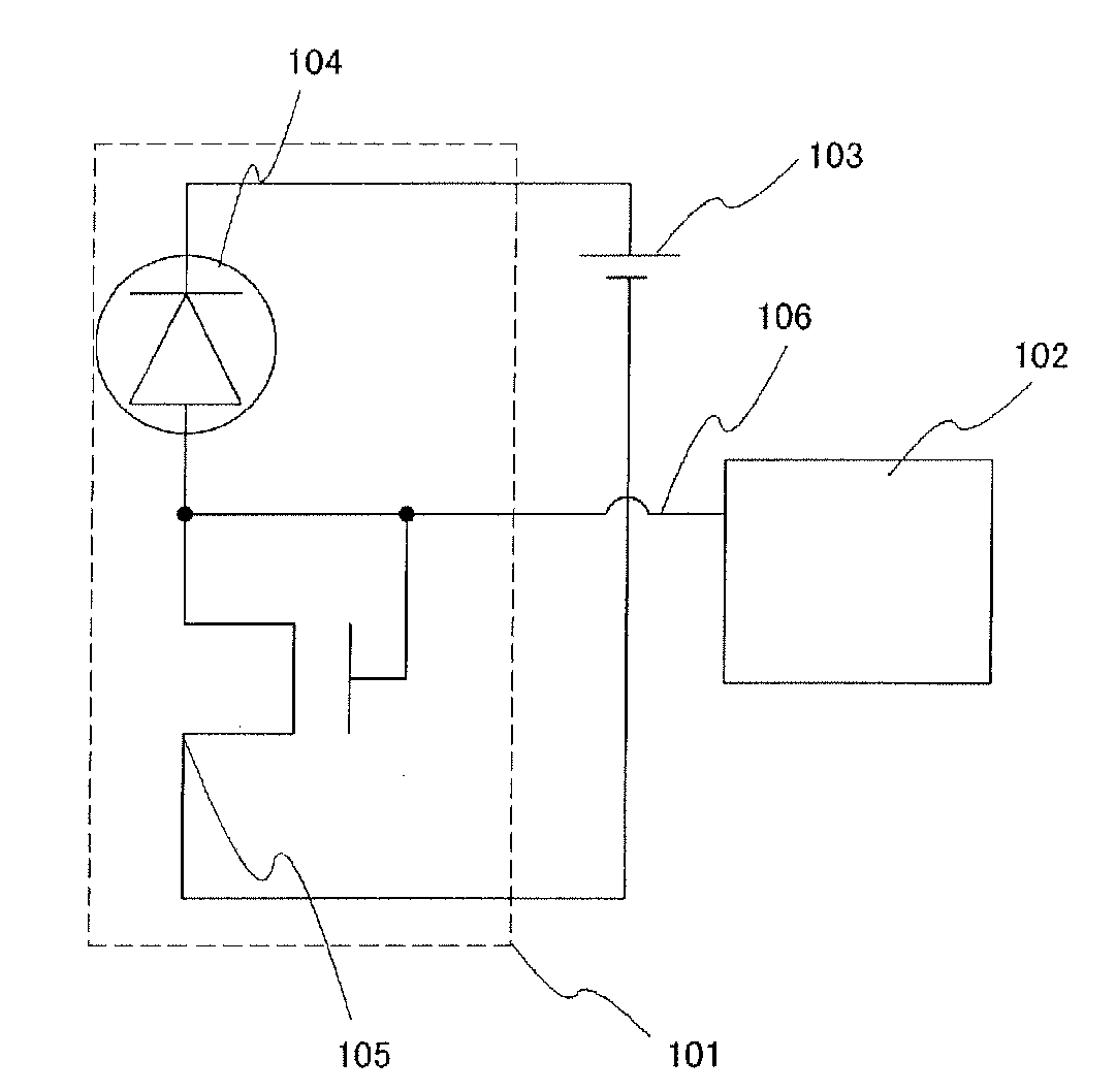
[0035]This embodiment mode will be described with reference to FIG. 1. A photoelectric conversion device shown in FIG. 1 includes a photoelectric conversion circuit 101, a voltage detection circuit 102, and a DC power supply 103. The photoelectric conversion circuit 101 includes a photoelectric conversion element 104 and an n-channel transistor 105. A first terminal (also referred to as an input terminal or a cathode) which is a cathode of the photoelectric conversion element 104 is connected to a high potential terminal (also referred to as a first terminal) of the DC power supply 103. In addition, a second terminal (also referred to as an output terminal or an anode) which is an anode of the photoelectric conversion element 104 is connected to a drain terminal and a gate terminal of the n-channel transistor 105. Note that the second terminal of the photoelectric conversion element 104 is connected to the voltage detection circuit 102 as an output terminal 106 of the photoelectric ...

embodiment mode 2

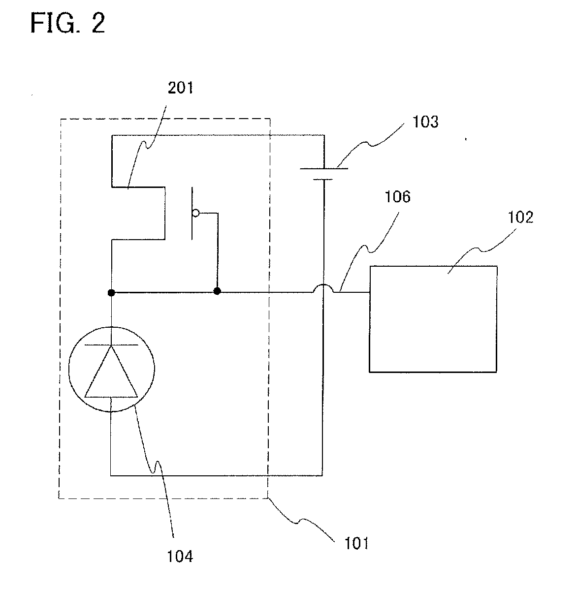
[0059]Embodiment Mode 2 of the present invention, which has a different structure from the photoelectric conversion device described in the above embodiment mode, will be described with reference to FIG. 6. A photoelectric conversion device described in this embodiment mode includes the photoelectric conversion circuit 101, the voltage detection circuit 102, and the DC power supply 103. The difference from the photoelectric conversion circuit described with reference to FIG. 1 in Embodiment Mode 1 is that the photoelectric conversion circuit 101 has a current amplifier 501 between the photoelectric conversion element 104 and the n-channel transistor 105. The first terminal which is a cathode of the photoelectric conversion element 104 is connected to the high potential terminal of the DC power supply 103. The second terminal which is an anode of the photoelectric conversion element 104 is connected to an input terminal of the current amplifier 501. An output terminal of the current ...

embodiment mode 3

[0066]Embodiment Mode 3 of the present invention will be described with reference to FIG. 9. This embodiment mode differs from the photoelectric conversion device of Embodiment Mode 1 in FIG. 1 in that a plurality of the n-channel transistors 105, such as the n-channel transistors 105-1, 105-2, 105-3, to 105-N (N is a natural number), are included in the photoelectric conversion circuit shown in this embodiment mode while one n-channel transistor 105 is included in the photoelectric conversion circuit in FIG. 1.

[0067]The n-channel transistor 105 is a circuit for converting the photocurrent I, into the output voltage Vout in the photoelectric conversion circuit 101, and the characteristics of the n-channel transistor 105 may vary due to various factors in the manufacturing steps in some cases. Even when the same amount of the photocurrent Ip is input, the level of the output voltage Vout changes due to the variation of the characteristics, and there is a possibility of a problem that...


PUM


Abstract

An output terminal of a photoelectric conversion element included in the photoelectric conversion device is connected to a drain terminal and a gate terminal of a MOS transistor which is diode-connected, and a voltage Vout generated at the gate terminal of the MOS transistor is detected in accordance with a current Ip which is generated at the photoelectric conversion element. The voltage Vout generated at the gate terminal of the MOS transistor can be directly detected, so that the range of output can be widened than a method in which an output voltage is converted into a current by connecting a load resistor, and so on.

Description

TECHNICAL FIELD[0001]The present invention relates to a photoelectric conversion device, and particularly relates to a photoelectric conversion device including thin film semiconductor elements. In addition, the present invention relates to electronic devices provided with the photoelectric conversion devices.BACKGROUND ART[0002]A number of photoelectric conversion devices used for detecting an electromagnetic wave are generally known, and for example, photoelectric conversion devices having sensitivity from ultra violet rays to infrared rays are collectively referred to as optical sensors. Among them, an optical sensor having sensitivity in a visible light region with a wavelength of 400 to 700 nm is particularly referred to as a visible light sensor, and a large number of visible light sensors are used for devices which need illuminance adjustment, on / off control, or the like depending on human living environment.[0003]In some display devices, ambient brightness of the display dev...

Claims


Application Information

Patent Timeline
IPC IPC(8): H01L31/113H01L31/10
CPCG01J1/4204H04N5/35518H01L27/14609G01J1/44H04N25/573
Inventor YANAGISAWA, MAKOTOHIROSE, ATSUSHI
Owner SEMICON ENERGY LAB CO LTD
Why Eureka
Try Eureka