Surface cleaning method of semiconductor wafer heat treatment boat
a technology of heat treatment boat and surface cleaning method, which is applied in the direction of surface treatment composition, decorative arts, chemistry apparatus and processes, etc., can solve the problems of low yield of semiconductor devices formed later on the wafer, metallic contamination of the wafer, and metallic contamination to diffuse outwardly, so as to prevent metallic contamination reduce the production time and manufacturing costs of the semiconductor wafer, and efficiently and easily remove metallic contamination
- Summary
- Abstract
- Description
- Claims
- Application Information
AI Technical Summary
Benefits of technology
Problems solved by technology
Method used
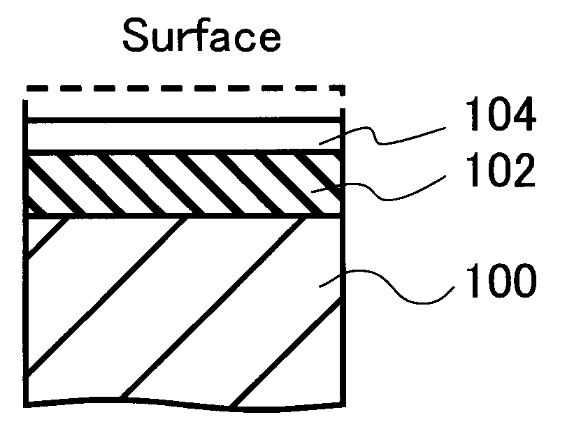
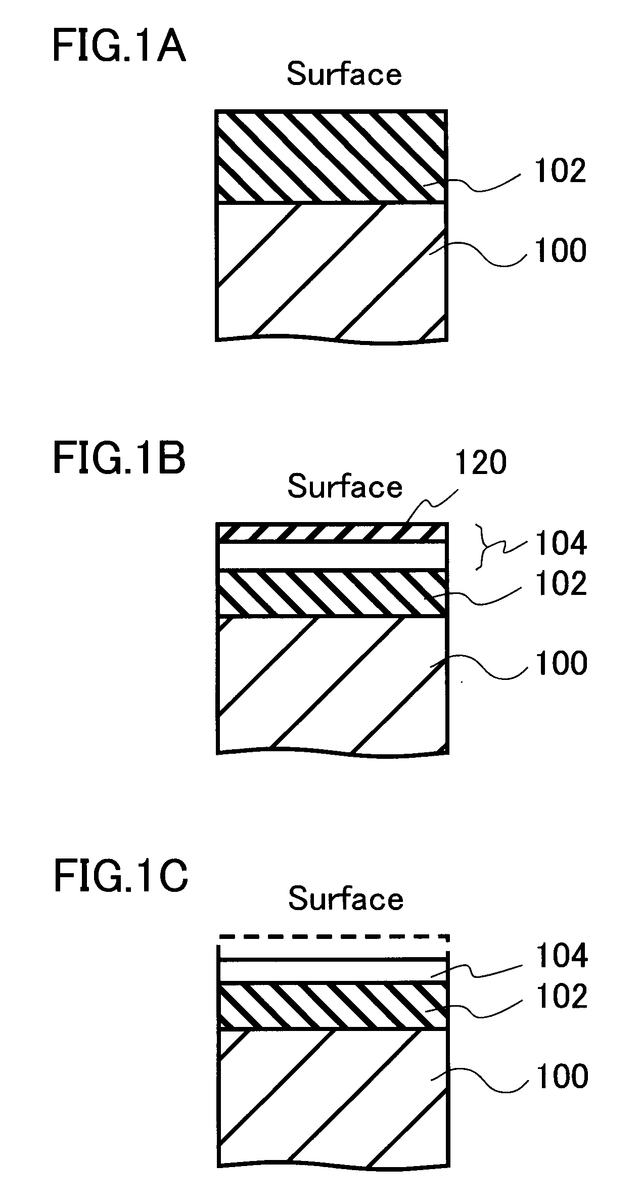
Image

Examples
example
[0038]Examples of the present invention will be described below, but the present invention is not limited to these examples.
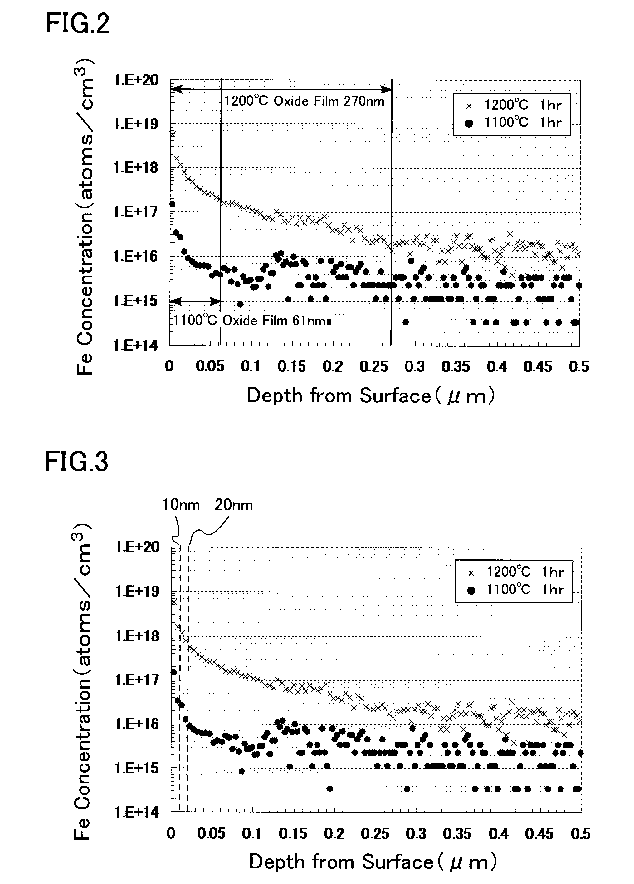
[0039]A semiconductor wafer heat treatment boat for semiconductor wafers of 300 mm in diameter formed from Si-impregnated SiC base material with CVD-SiC deposited on the surface thereof was dry-oxidized at 1200° C. for one hour. An oxide film of about 270 nm was formed on the boat surface by the oxidation. The boat was soaked in a 0.5% HF solution for 2 min to remove the oxide film of up to about 10 nm depth from the surface of the oxide film by etching.
[0040]50 silicon wafers were loaded on the boat that underwent the above surface cleaning treatment to heat-treat the silicon wafers in an argon gas atmosphere at 1200° C. for one hour. After the heat treatment, the average Fe concentration of three silicon wafers at the wafer support position by the boat was measured by the SPV (Surface Photo Voltage) method. FIG. 5 shows a measurement result.
[0041]The conditio...
PUM
| Property | Measurement | Unit |
|---|---|---|
| Temperature | aaaaa | aaaaa |
| Temperature | aaaaa | aaaaa |
| Fraction | aaaaa | aaaaa |
Abstract
Description
Claims
Application Information
 - R&D
- Intellectual Property
- Life Sciences
- Materials
- Tech Scout
- Unparalleled Data Quality
- Higher Quality Content
- 60% Fewer Hallucinations
Browse by: Latest US Patents, China's latest patents, Technical Efficacy Thesaurus, Application Domain, Technology Topic, Popular Technical Reports.
© 2025 PatSnap. All rights reserved.Legal|Privacy policy|Modern Slavery Act Transparency Statement|Sitemap|About US| Contact US: help@patsnap.com