Semiconductor integrated circuit and design method of signal terminals on input/output cell

a technology of integrated circuits and signal terminals, applied in the direction of instruments, program control, basic electric elements, etc., can solve the problems of interconnection wiring, open failure of vias b, and limitations on the layout of vias b>, so as to suppress the increase in the area of semiconductor chips, suppress the increase in the cost of semiconductor integrated circuits, and eliminate or reduce the migration of atoms

Inactive Publication Date: 2008-09-25
PANASONIC CORP
View PDF6 Cites 0 Cited by
  • Summary
  • Abstract
  • Description
  • Claims
  • Application Information

AI Technical Summary

Benefits of technology

[0010]An object of the present invention is to provide a semiconductor integrated circuit including input / output cells having signal terminals thereon in which an open failure of a via is effectively prevented by employing a connection architecture between the signal terminals on the input / output cells and the interconnect wirings that is different from the connection architecture shown in FIG. 10, with which an open failure of a via occurs due to the migration of atoms.
[0029]Thus, according to the present invention, a signal terminal on an I / O cell includes a plurality of conductive layers, wherein the width of the broadest one of the plurality of conductive layers is limited to such a width that only one largest-diameter via can be accommodated. Therefore, with an interconnect wiring connected to any one of the plurality of conductive layers, the connection architecture is no longer a connection architecture that results in an open failure of a via due to the migration of atoms as shown in FIG. 10, thereby eliminating or reducing the migration of atoms from the interconnect wiring into one of the conductive layers of the signal terminal. As a result, vias can be freely arranged on the interconnect wiring, thus causing no restrictions in designing the layout of the vias and interconnect wirings. Thus, it is possible to suppress the increase in the area of the semiconductor chip and suppress the increase in the cost of the semiconductor integrated circuit.

Problems solved by technology

The miniaturization of semiconductor integrated circuits and the transition of wiring materials thereof have led to a new problem as follows.
The migration of atoms may deteriorate the connection between the via 42 and the narrow branch wiring 41, resulting in a near disconnection therebetween and causing an open failure of the via 42.
However, these methods impose limitations on the layout of the vias 32 and the interconnect wirings.
Since signal wirings in the semiconductor chip C are routed very closely together, such layout limitations will increase the total area of the semiconductor chip C and the cost of the semiconductor integrated circuit.
Apparently, the level of miniaturization will further advance, and the open failure of a via due to the migration of atoms will accordingly become a more serious issue in the future.

Method used


Image

  • Semiconductor integrated circuit and design method of signal terminals on input/output cell
  • Semiconductor integrated circuit and design method of signal terminals on input/output cell
  • Semiconductor integrated circuit and design method of signal terminals on input/output cell

Examples


first embodiment

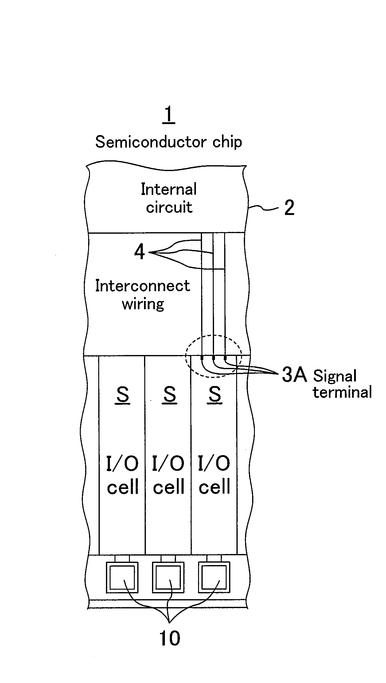
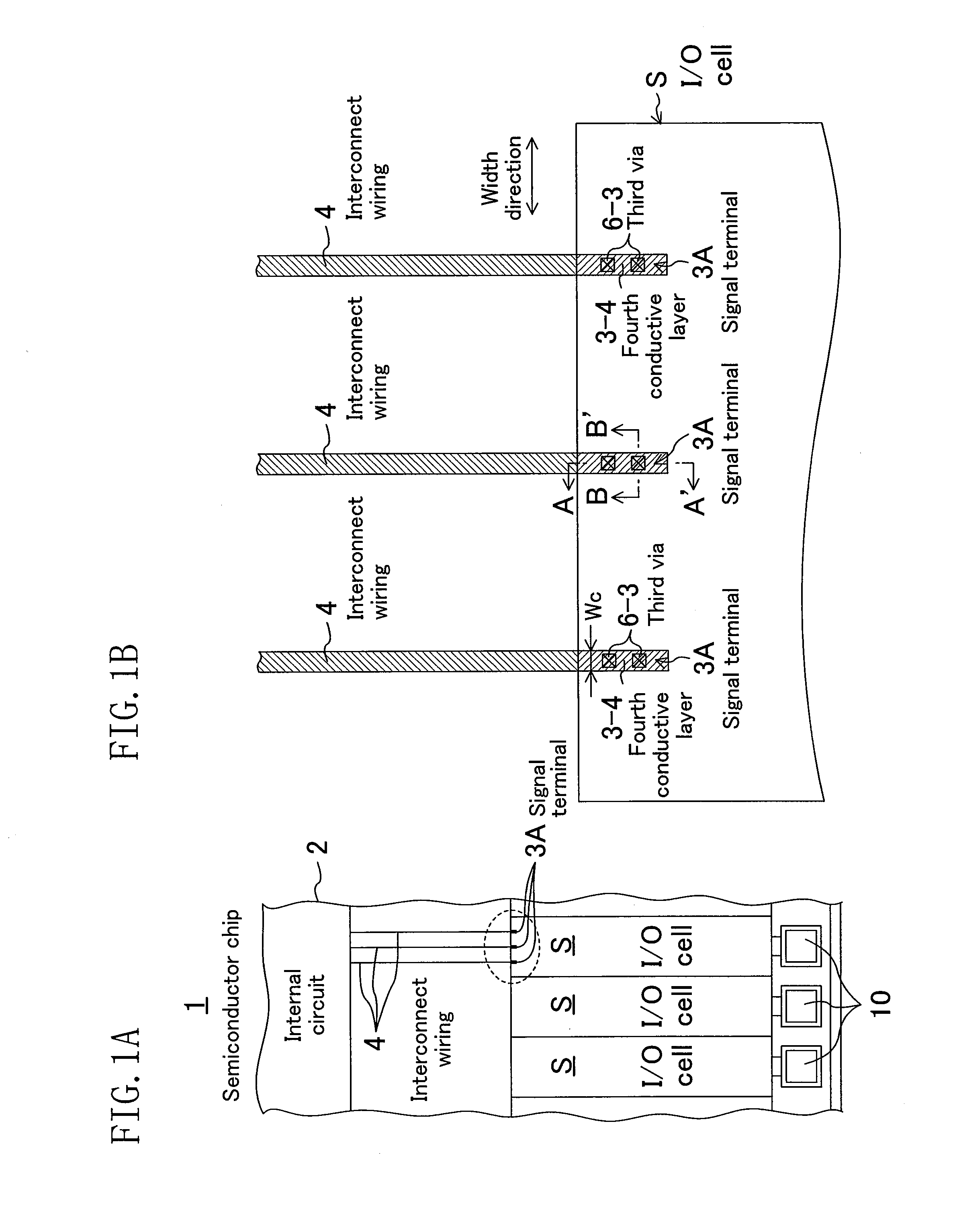
[0044]FIGS. 1A and 1B are plan views showing a semiconductor integrated circuit according to a first embodiment of the present invention.

[0045]Referring to FIG. 1A, a semiconductor chip 1 is a semiconductor integrated circuit employing a standard cell architecture. An internal circuit 2 including a signal processing circuit, etc., is provided within the semiconductor chip 1, with many I / O cells S being arranged in parallel to one another along the periphery of the semiconductor chip 1. Each I / O cell S is connected to the internal circuit 2 by interconnect wirings 4. Signals are input to, and output from, the I / O cells S via an electrode bump 10, which is provided at the peripheral end of each the I / O cell S. Each cell S is not limited to a cell capable of both inputting and outputting signals, but may be a cell only capable of either inputting or outputting signals. Such input cells, output cells and input / output cells are herein referred to collectively as I / O cells.

[0046]The conne...

second embodiment

[0058]A second embodiment of the present invention will now be described.

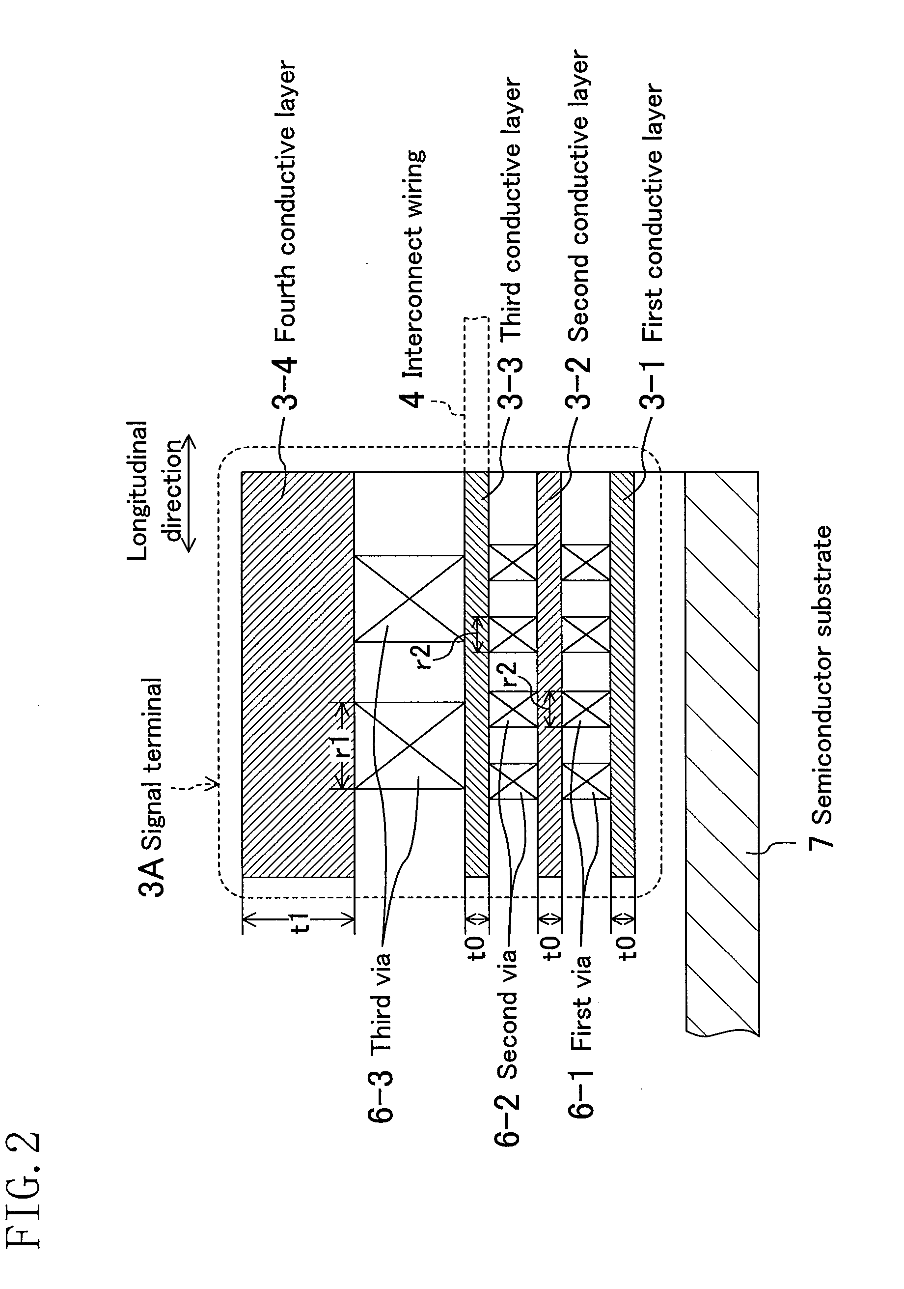
[0059]FIG. 6 is a cross-sectional view taken in the direction corresponding to line B-B′ of FIG. 1B (i.e., a cross-sectional view in the width direction of the signal terminal 3A), showing a semiconductor integrated circuit according to the second embodiment of the present invention. The present embodiment differs from the first embodiment shown in FIG. 3A in that a plurality of (two in the illustrated example) each of the first and second vias (the vias other than the largest-diameter via) 6-1 and 6-2 are arranged in the width direction of the signal terminal 3A.

[0060]Although only one each of the first via 6-1 and the second via 6-2 is provided in the width direction of the signal terminal 3A in the example shown in FIG. 3A, the diameter of the first via 6-1 and the second via 6-2 is smaller than that of the third via (the largest-diameter via) 6-3, and therefore a plurality of such vias may be provided in th...

third embodiment

[0062]A third embodiment of the present invention will now be described.

[0063]FIG. 7A is a cross-sectional view taken in the direction corresponding to line B-B′ of FIG. 1B (i.e., a cross-sectional view in the width direction of the signal terminal 3A), showing a semiconductor integrated circuit according to the third embodiment of the present invention. The present embodiment differs from the first embodiment shown in FIGS. 3A to 3C in that only the third and fourth conductive layers 3-3 and 3-4 are the broadest conductive layer, with the first and second conductive layers (conductive layers other than the broadest conductive layers) 3-1 and 3-2 being formed with a width smaller than that of the third and fourth conductive layers (the broadest conductive layers) 3-3 and 3-4.

[0064]Specifically, the first and second conductive layers 3-1 and 3-2 are formed with the same width as the third and fourth conductive layers 3-3 and 3-4 in the example shown in FIG. 3A. In contrast, in the ex...


PUM


Abstract

A semiconductor integrated circuit, including an input / output cell including signal terminals, wherein the signal terminal of the input / output cell is connected to an internal circuit via an interconnect wiring. The signal terminal of the I / O cell includes a plurality of (e.g., four) conductive layers. Each pair of adjacent ones of the plurality of conductive layers are connected together by a via. One of the plurality of conductive layers to which a via of the largest diameter is connected (e.g., the fourth conductive layer) is formed with a width such that only one of the largest-diameter via can be accommodated. Therefore, it is possible to suppress the migration of atoms from the interconnect wiring to the input terminal of the I / O cell, and to suppress the open failure of the via formed on the interconnect wiring.

Description

CROSS REFERENCE TO RELATED APPLICATIONS[0001]This Non-provisional application claims priority under 35 U.S.C. §119(a) on Patent Application No. 2007-074828 filed in Japan on Mar. 22, 2007, the entire contents of which are hereby incorporated by reference.BACKGROUND OF THE INVENTION[0002]The present invention relates to a semiconductor integrated circuit employing a standard cell architecture, and more particularly to the structure of signal terminals on input / output cells.[0003]FIG. 9A shows a part of a conventional semiconductor integrated circuit employing a standard cell architecture, in which an internal circuit I including a signal processing circuit, etc., is provided within a semiconductor chip C, with many input / output cells 30 being arranged in parallel to one another along the periphery of the semiconductor chip C. Each input / output cell 30 is connected to the internal circuit I by interconnect wirings 31. Signals are input to, and output from, the input / output cells 30 vi...

Claims


Application Information

Patent Timeline
Patent Type & Authority Applications(United States)
IPC IPC(8): H01L23/48G06F9/45
CPCH01L23/5226H01L23/5283H01L2924/0002H01L2924/00
Inventor GION, MASAHIRO
Owner PANASONIC CORP
Why Eureka
Try Eureka