


Quick Research
Generate reliable direction feasibility study reports for your R&D in just a few steps.

Technical Q&A
Discover and master advanced knowledge NOW. Basics, ideas, possibilities, all at once.

Find Solutions
As an expert in R&D theories, this can generate solutions to your technical problems instantly.

Evaluate Feasibility
Analyze your overall solution with one click, know your potential R&D risks in advance.

Monitor Landscape
Get weekly tech updates, stay abreast of the latest tech innovations and key insights.
Semiconductor protection circuit, method for fabricating the same and method for operating semiconductor protection circuit
- Summary
- Abstract
- Description
- Claims
- Application Information
AI Technical Summary
Benefits of technology
Problems solved by technology
Method used
Image

Examples
embodiment 1
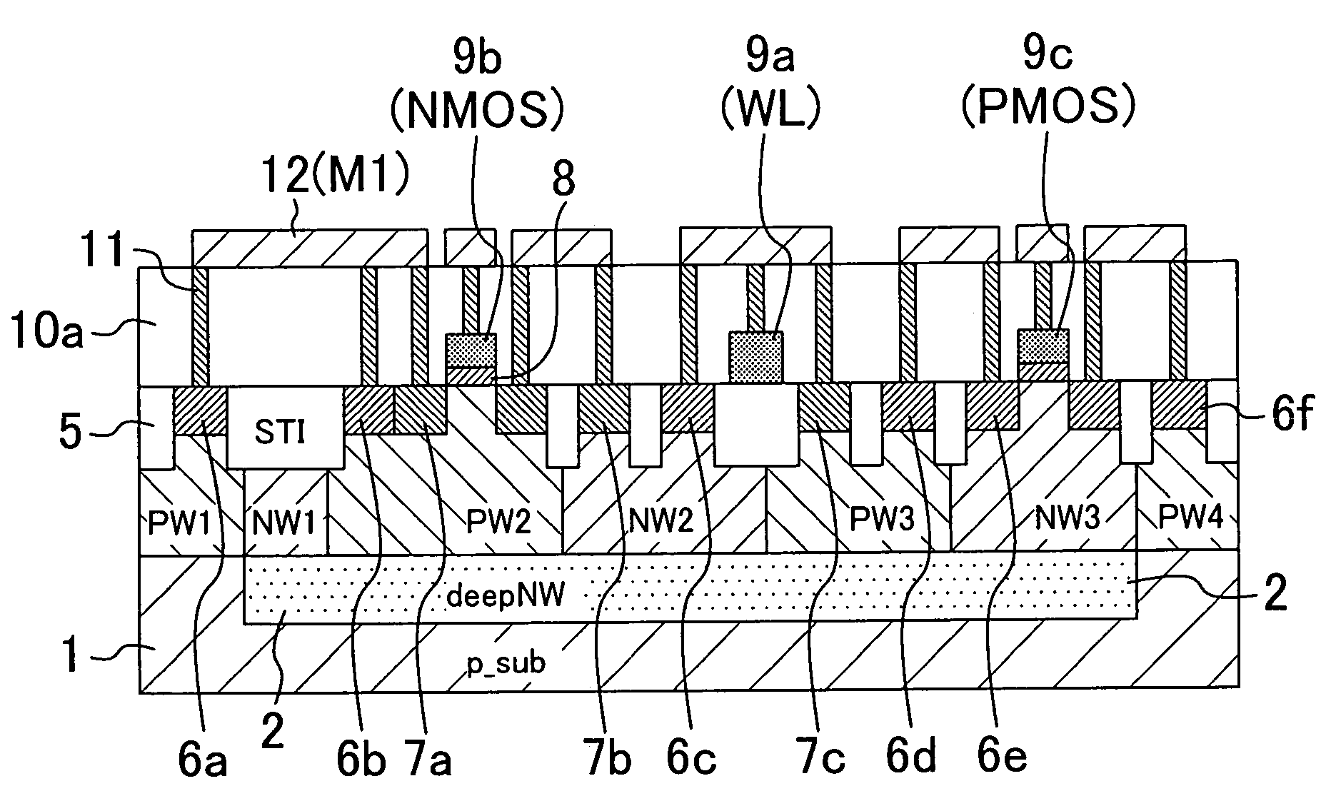
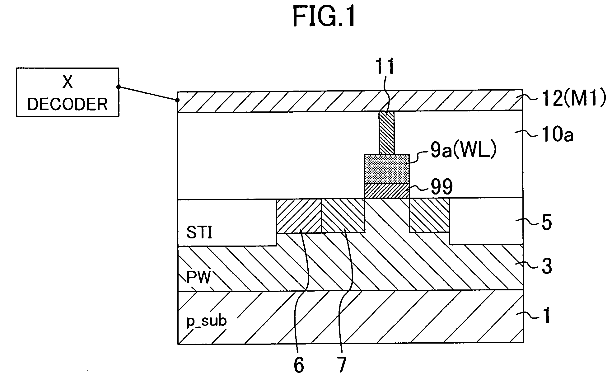
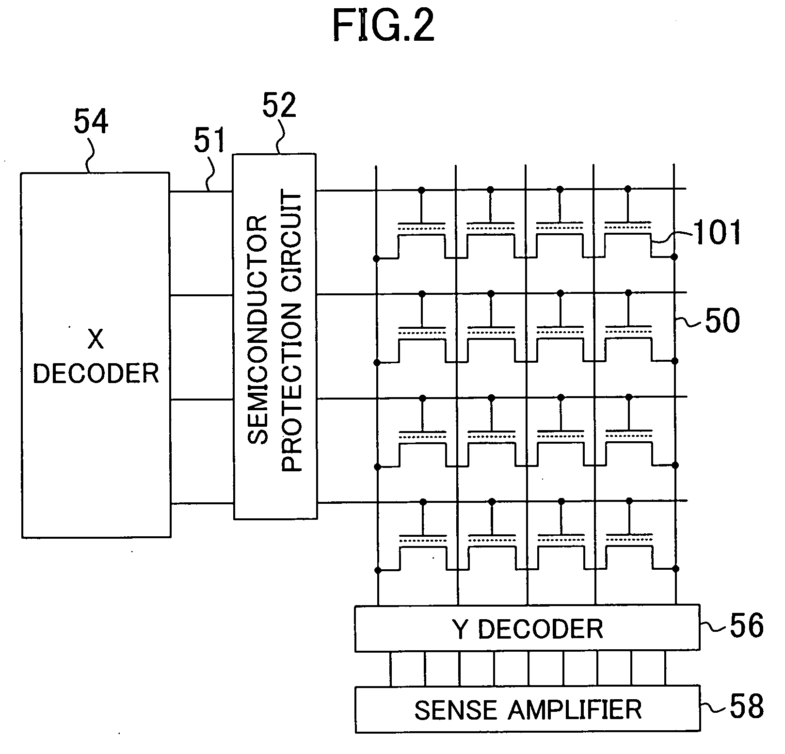
[0043]FIG. 1 is a cross-sectional view of a memory cell of a MONOS semiconductor memory according to Embodiment 1 of the invention, and FIG. 2 is a circuit diagram of a memory cell array of the semiconductor memory of this embodiment. Also, FIG. 3 is a circuit diagram for schematically showing a semiconductor protection circuit of the semiconductor memory of this embodiment in a state attained during the fabrication.
[0044]As shown in FIG. 2 the semiconductor memory of this embodiment includes a plurality of memory cells 101 arranged in the form of a matrix; word lines 51 provided correspondingly to respective rows of the memory cells 101 to be connected to gate electrodes of MONOS structures of the memory cells 101; bit lines 50 provided correspondingly to respective columns to be connected to N-type diffusion layers 7 of the memory cells 101; an X decoder 54 for driving the word lines 51; a Y decoder 56 connected to the respective bit lines 50; a sense amplifier 58 for amplifying a...
embodiment 2
[0073]FIG. 12 is a circuit diagram of a semiconductor protection circuit according to Embodiment 2 of the invention. FIG. 12 shows a state of the semiconductor protection circuit attained, for example, during formation of a first layer metal interconnect.
[0074]The semiconductor protection circuit of this embodiment includes, in addition to the structure of the semiconductor protection circuit of Embodiment 1 shown in FIG. 4, a third antenna 208 connected to an N-type well. The third antenna 208 is made of an interconnect disposed on the same interconnect layer as an NMIS gate antenna 206 and a PMIS gate antenna 207 (for example, made of the first layer metal interconnect).
[0075]Owing to this structure, charge generated in forming interconnects enters a node between a forward diode 202 and the drain of an NMIS 204 from the third antenna 208. Accordingly, in the case where positive charge enters the third antenna 208 during the fabrication, the positive charge is drained to the ground...
PUM
 Abstract
Description
Claims
Application Information
 - R&D Engineer
- R&D Manager
- IP Professional
- Industry Leading Data Capabilities
- Powerful AI technology
- Patent DNA Extraction
Browse by: Latest US Patents, China's latest patents, Technical Efficacy Thesaurus, Application Domain, Technology Topic, Popular Technical Reports.
© 2024 PatSnap. All rights reserved.Legal|Privacy policy|Modern Slavery Act Transparency Statement|Sitemap|About US| Contact US: help@patsnap.com