
Solid-state imaging device and imaging apparatus

a technology of solid-state imaging and imaging apparatus, which is applied in the direction of radio frequency controlled devices, television systems, instruments, etc., can solve the problems of limited frame rate, increase in conversion processing speed, so as to reduce the time necessary for comparison processing in the comparing unit, the effect of increasing the speed of ad conversion processing

Inactive Publication Date: 2008-08-14
SONY CORP
View PDF4 Cites 53 Cited by
  • Summary
  • Abstract
  • Description
  • Claims
  • Application Information

AI Technical Summary

Benefits of technology

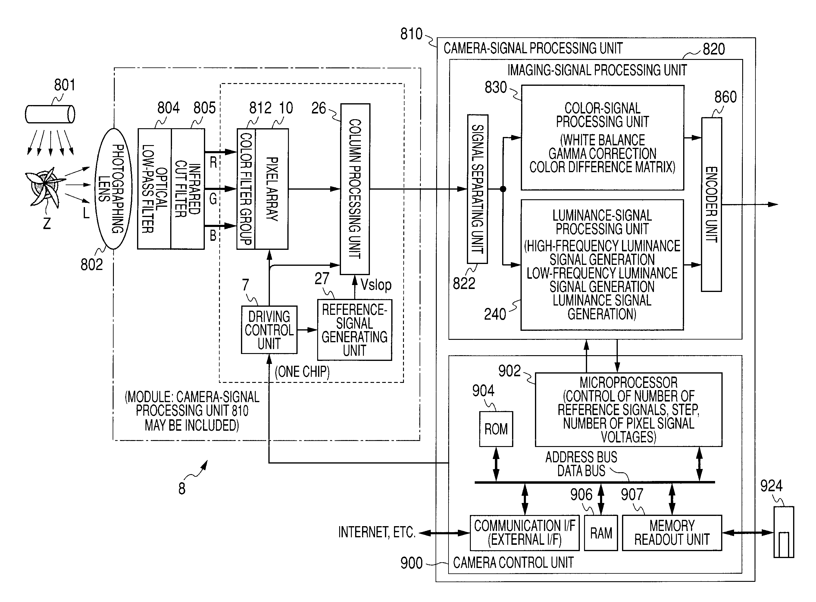
[0011]A MOS (CMOS)) type image sensor, which is one of the solid-state imaging devices, converts, for each of pixels, an electric charge into an electric signal making use of a characteristic that the image sensor can be manufactured in a process same as that for a MOS (CMOS) integrated circuit and processes, for each of columns and in parallel, the electric signal read out from the pixel. In this way, it is possible to improve processing speed compared with an image sensor that is not a column parallel type.
[0012]If AD conversion of the column parallel type is applied as processing for an electric signal, it is possible to improve AD conversion speed compared with speed of AD conversion that is not the column parallel type. In other words, to realize a further increase in speed of AD conversion, an increase in speed of a circuit for AD-converting the electric signal for each of columns is necessary.
[0016]Therefore, it is desirable to provide a mechanism that can realize, when the AD conversion system of the reference signal comparison type is adopted, an increase in speed of AD conversion processing and a reduction in power consumption by reducing time necessary for the comparison processing in the comparing unit while controlling an increase in the circuit area.
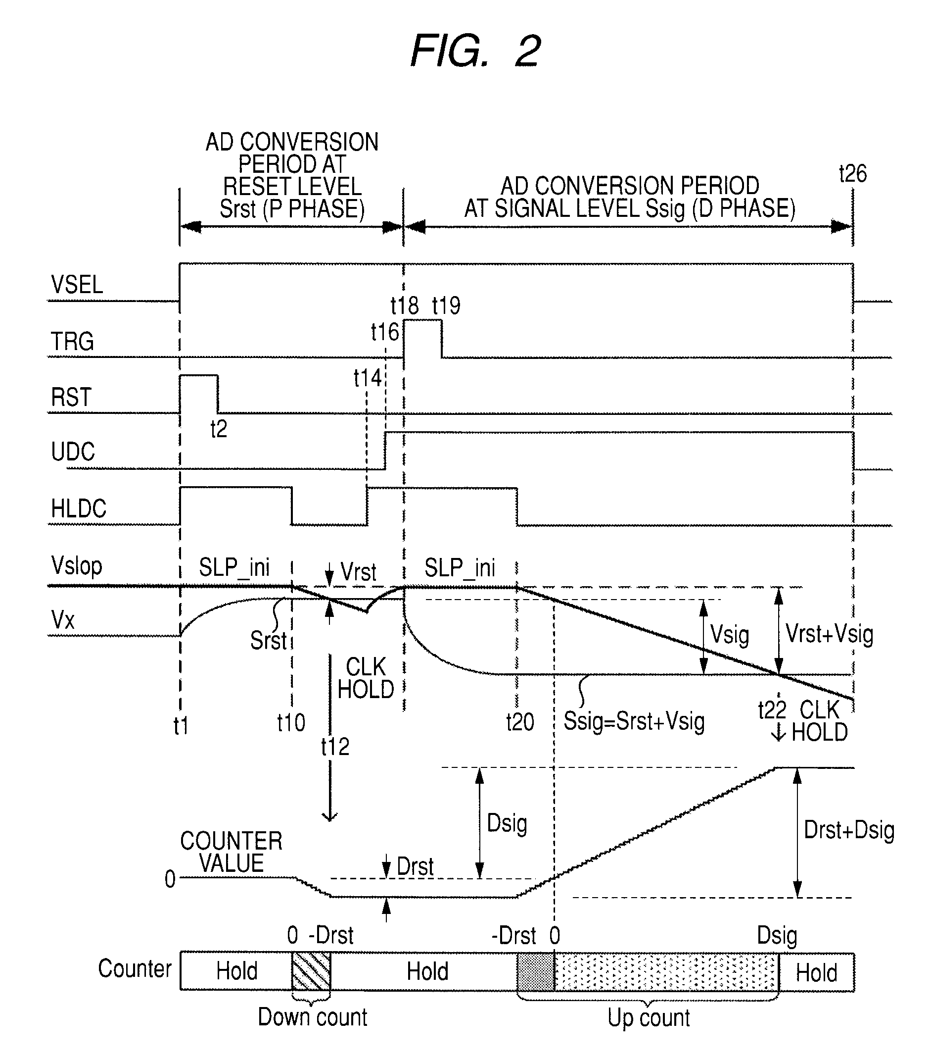
[0030]In the first mechanism of the present invention, AD conversion with resolution of 1 LSB maintained is performed by preparing plural kinds of reference signals, a level difference between adjacent ones of which is fixed, comparing the reference signals with an identical pixel signal, and correcting, on the basis of results of the comparison, a count value stored during the comparison of any one of the reference signals. The plural kinds of reference signals having different levels corresponding to an identical count value are matched and compared with one pixel signal. Therefore, it is possible to reduce comparison processing time in performing AD conversion with resolution of 1 LSB secured to time obtained by dividing processing time of comparison processing for one reference signal and one pixel signal by the number of reference signals. Since time necessary for the comparison processing in the comparing unit is reduced, it is possible to realize an increase in speed of AD conversion processing and a reduction in power consumption.
[0031]In the second mechanism of the present invention, AD conversion with resolution of 1 LSB maintained is performed by dividing pixel signals from pixels into k kinds of pixel signals, a level difference between adjacent ones of which is 1 LSB, comparing the pixel signals with one reference signal that changes stepwise at a rate of change of k LSB, and correcting, on the basis of results of the comparison, a count value stored during the comparison of any one of the pixel signals. The plural kinds of pixel signals, a level difference between adjacent ones of which is 1 LSB, are matched and compared with one reference signal. Therefore, it is possible to reduce comparison processing time in performing AD conversion with resolution of 1 LSB secured to time obtained by dividing processing time of comparison processing of one reference signal and one pixel signal by the number of reference signals. Since time necessary for the comparison processing in the comparing unit is reduced, it is possible to realize an increase in speed of AD conversion processing. Conversely, when processing speed same as that when the first or second mechanism is not applied is maintained, it is possible to reduce power consumption if the first or second mechanism is applied.
[0032]In both the first and second mechanisms, rather than providing plural AD conversion units, it is sufficient to prepare plural reference signals or pixel signals and provide a selecting unit that switches the reference signals or the pixel signals and a mechanism for controlling operations of the respective units in association with one another. Therefore, it is possible to realize an increase in speed of AD conversion processing and a reduction in power consumption.

Problems solved by technology

Therefore, time necessary for comparison processing in the comparing unit poses a problem in AD conversion performance; in particular, an increase in speed of conversion processing and a frame rate is limited.

Method used


Image

  • Solid-state imaging device and imaging apparatus
  • Solid-state imaging device and imaging apparatus
  • Solid-state imaging device and imaging apparatus

Examples


first example of first embodiment

[0167]FIGS. 4 to 6 are diagrams for explaining AD conversion processing of a reference signal comparison type according to a first example of a first embodiment of the present invention. FIG. 4 is a circuit block diagram for explaining an example of the structure around the reference-signal control unit 25 applied to the AD conversion processing of the reference signal comparison type according to the first example of the first embodiment. FIGS. 5A and 5B are functional block diagrams for explaining details of the DA converter 27a applied to respective kinds of AD conversion processing of the reference signal comparison type according to the first example of the first embodiment and a comparative example. FIG. 6 is a diagram for explaining an operation principle of the AD conversion processing of the reference signal comparison type according to the first example of the first embodiment and shows a relation between two kinds of reference signals Vslop_1 and Vslop_2 and the pixel sig...

third example of first embodiment

[0206]FIG. 9 to FIGS. 11A and 11B are diagrams for explaining AD conversion processing of a reference signal comparison type according to a third example of the first embodiment. FIG. 9 is a circuit block diagram for explaining an example of the structure around the reference-signal control unit 25 applied to the AD conversion processing of the reference signal comparison type according to the third example of the first embodiment. FIG. 10 is a functional block diagram for explaining details of the DA converter 27a applied to the AD conversion processing of the reference signal comparison type according to the third example of the first embodiment. FIGS. 11A and 11B are diagrams for explaining an operation principle of the AD conversion processing of the reference signal comparison type according to the third example of the first embodiment and show a relation between four kinds of reference signals Vslop_1, Vslop_2, Vslop_3, and Vslop_4 and the pixel signal voltage Vx.

[0207]In the ...

fourth example of first embodiment

Generalization

[0234]FIG. 12 is a diagram for explaining AD conversion processing of a reference signal comparison type according to a fourth example of the first embodiment and shows M kinds of reference signals Vslop.

[0235]Plural kinds of reference signals Vslop, a voltage difference between adjacent one of which is 1 LSB, are used. In the first example, an AD conversion period is reduced to a half by changing the reference signals Vslop in a 2 LSB step. In the third example, an AD conversion period is reduced to a quarter by changing the reference signals Vslop in a 4 LSB step. By developing the forms of these examples, eventually, as a processing form of the first embodiment, an AD conversion period can be reduced to ½̂n by using plural kinds of reference signals Vslop, a voltage difference between adjacent ones of which is 1 LSB, and that change stepwise, and setting a minimum step width of the reference signals Vslop based on the count clock CKdac to 2̂n LSB (n is a positive in...


PUM


Abstract

A solid-state imaging device includes a reference-signal generating unit that generates plural kinds of reference signals for converting an analog pixel signal into digital data, a reference-signal selecting unit that selects any one of the plural kinds of reference signals, a comparing unit that compares the pixel signal and the selected reference signal, and a count unit that performs count processing in parallel with comparison processing in the comparing unit and stores a count value at a point when the comparison processing is completed. The count unit decides digital data of the pixel signal in a 1 LSB step by storing a count value at a point when the comparison processing is completed for any one of the plural kinds of reference signals and correcting the stored count value on the basis of results of the comparison processing for respective remaining reference signals of the plural kinds of reference signals.

Description

CROSS-REFERENCES TO RELATED APPLICATIONS[0001]The present invention contains subject matter related to Japanese Patent Application JP 2007-031889 filed in the Japanese Patent Office on Feb. 13, 2007, the entire contents of which being incorporated herein by reference.BACKGROUND OF THE INVENTION[0002]1. Field of the Invention[0003]The present invention relates to a solid-state imaging device, which is an example of a semiconductor device for detecting a physical quantity distribution, and an imaging apparatus. More specifically, the present invention relates to a mechanism that is formed by arraying plural unit components, which have sensitivity to electromagnetic waves inputted from the outside such as light and radiations, and outputs an electric signal indicating a physical quantity distribution converted into an electric signal by the unit components to the outside.[0004]2. Description of the Related Art[0005]In recent years, as examples of a solid-state imaging device, image sen...

Claims


Application Information

Patent Timeline
IPC IPC(8): H04N5/228H01L27/146H03M1/56H04N5/335H04N5/341H04N5/374H04N5/376H04N5/378
CPCH04N5/378H04N5/335H04N25/00H04N25/78H04N25/75
Inventor SAKAI, NAOFUMIMORI, TOMONORI
Owner SONY CORP
Learn More