
Semiconductor device and shift register circuit

a technology of shift register and semiconductor device, which is applied in the direction of digital storage, pulse automatic control, instruments, etc., can solve the problems of circuit malfunction, similar vth shift problem in organic transistor, etc., and achieve the effect of preventing circuit malfunction of semiconductor devi

Active Publication Date: 2008-08-07
TRIVALE TECH
View PDF2 Cites 109 Cited by
  • Summary
  • Abstract
  • Description
  • Claims
  • Application Information

AI Technical Summary

Benefits of technology

[0008]An object of the present invention is to provide a transistor capable of suppressing the negative shift of threshold voltage, thereby preventing malfunctions of a semiconductor device including a shift register.
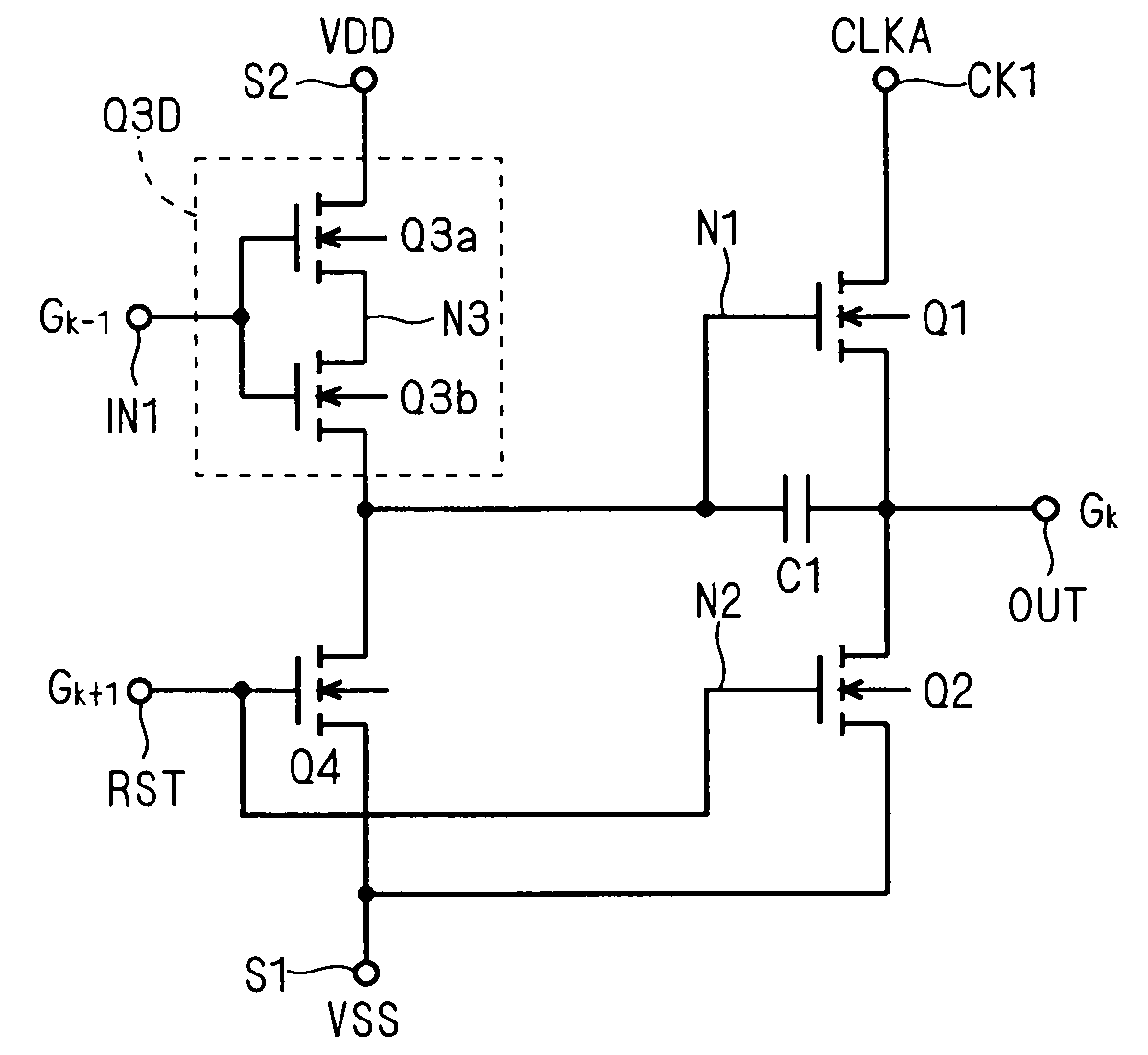
[0011]According to the semiconductor device of the present invention, the potential condition where both the source and drain are at the H level and the control electrode is at the L level is prevented from occurring in each of the transistors connected in series, which prevents the threshold voltage of the transistors from shifting in the negative direction. Accordingly, each transistor is turned off (brought into the cut-off state) with reliability when the control electrode is brought into the L level, which prevents the semiconductor device from malfunctioning.
[0012]According to the shift register of the present invention, the potential condition where both the source and drain are at the H level and the control electrode is at the L level is prevented from occurring in each of the transistors constituting the charging circuit for the control electrode of the first transistor, which prevents the threshold voltage of the transistors from shifting in the negative direction. Accordingly, the charging circuit is turned off (brought into the cut-off state) with reliability when the control electrode of the charging circuit is brought into the L level, preventing the first transistor from turning on unnecessarily, which prevents the shift register from malfunctioning.

Problems solved by technology

It is known that this Vth shift problem similarly occurs in organic transistors, not only in a-Si transistors.
That is, the a-Si transistor cannot interrupt current completely, which causes malfunctions of the circuit.
In the normal operation of the shift register as will be described later in detail, the charging transistor is in the aforementioned potential condition (where the gate of the transistor has a lower potential than both the drain and source) for a certain period of time, disadvantageously causing the negative shift of threshold voltage, which results in malfunctions.

Method used


Image

  • Semiconductor device and shift register circuit
  • Semiconductor device and shift register circuit
  • Semiconductor device and shift register circuit

Examples


first preferred embodiment

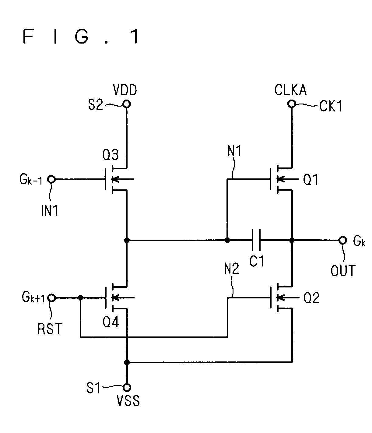
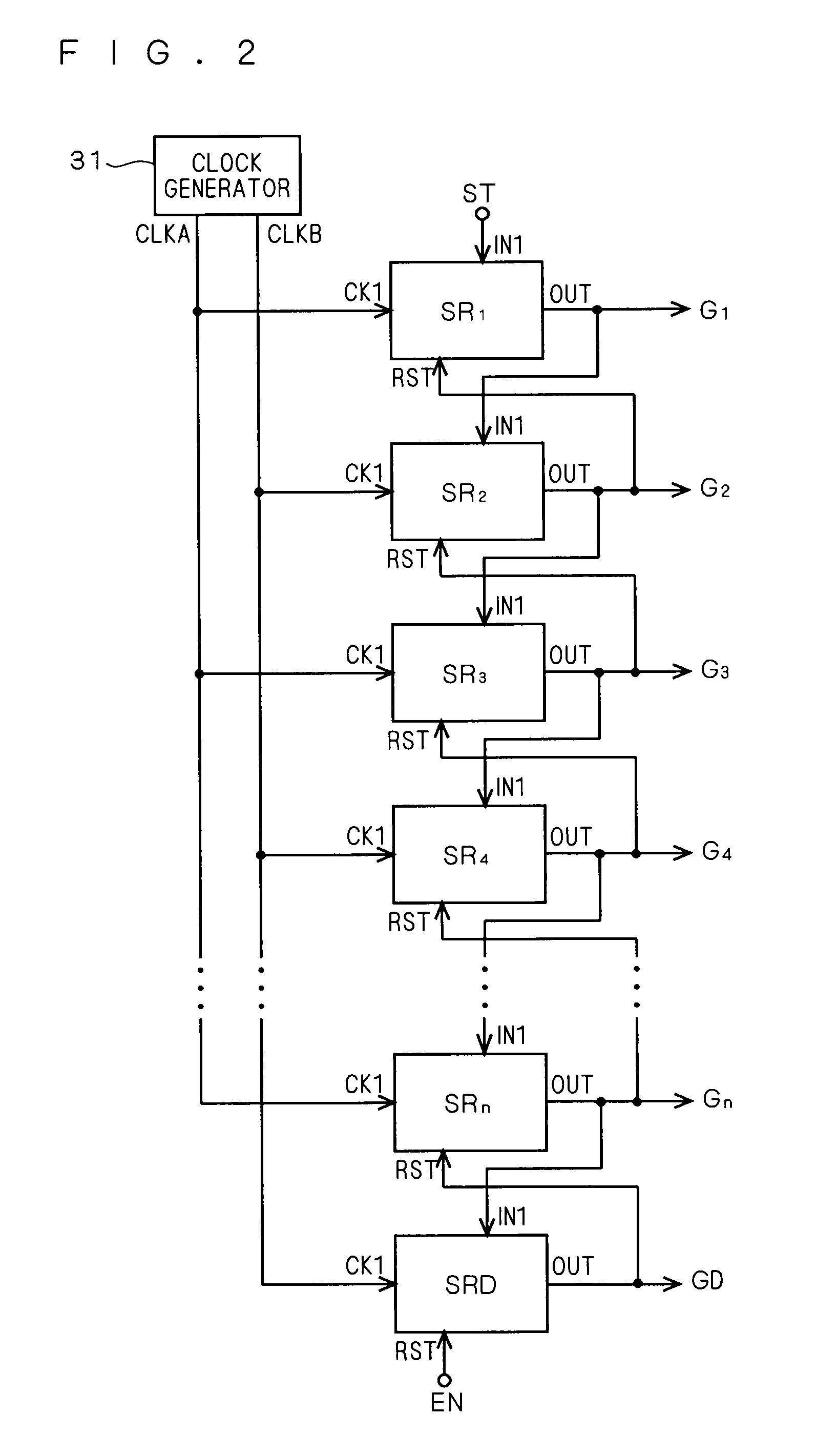
[0040]For ease of description of the present invention, a conventional shift register will be described first. Typically, the shift register has a multistage structure made up of a plurality of shift registers connected in cascade (cascade-connected). Throughout the present specification, each of the shift registers constituting the multistage shift register will be called “a unit shift register”.

[0041]As described earlier, the shift register can be used as a gate-line driving circuit of a display apparatus. A specific configuration of a display apparatus employing a shift register as the gate-line driving circuit is disclosed in, e.g., Japanese Patent Application Laid-Open No. 2006-277860 made by the inventors of the present application (FIGS. 1, 2, etc). The following description will be made assuming that the low supply voltage (VSS) as a reference potential of the circuit is 0V; in a practical display apparatus, however, a reference potential is determined with reference to a vo...

second preferred embodiment

[0090]A specific example of a shift register to which the dual-gate transistor according to the present invention may be applied will be described.

[0091]FIG. 11 is a circuit diagram of a unit shift register SR according to a second preferred embodiment. The unit shift register SR includes an inverter added to the circuit shown in FIG. 7, where the node N1 (gate of transistor Q1) serves as its input node and the node N2 (gate of transistor Q2) serves as its output node. That is, the gate of the transistor Q2 (node N2) is not connected to the reset terminal RST, unlike the circuit shown in FIG. 7.

[0092]The inverter is made up of a transistor Q5 diode-connected between the node N2 and second power terminal S2 and a transistor Q6 connected between the node N2 and first power terminal S1 having its gate connected to the node N1. The on-state resistance of the transistor Q6 is set sufficiently smaller than that of the transistor Q5.

[0093]Since the transistor Q6 turns off when the node N1 ...

third preferred embodiment

[0097]FIG. 12 is a circuit diagram of a unit shift register SR according to a third preferred embodiment. The unit shift register SR includes a transistor Q7 having its gate connected to the node N2 additionally provided between the node N1 and first power terminal S1 in the circuit shown in FIG. 11. That is, the transistor Q7 has a gate electrode connected to the node N2 and is intended to discharge the node N1.

[0098]In the unit shift register SRk shown in FIG. 11, the transistor Q4 turns on to discharge the node N1 when the output signal Gk+1 from the immediately succeeding stage rises to the H level (in the selected period of the succeeding stage), but the node N1 is at the L level with high impedance (floating state) in the other non-selected period. The node N1 therefore rises in level when supplied with charges by noise or leak current in the non-selected period. Then, the malfunction occurs in which the transistor Q1 turns on and output signal G is output as an error signal.

[...


PUM


Abstract

A dual-gate transistor formed of two transistors connected in series between a first power terminal and a first node is used as a charging circuit for charging a gate node (first node) of a transistor intended to pull up an output terminal of a unit shift register. The dual-gate transistor is configured such that the connection node (second node) between the two transistors constituting the dual-gate transistor is pulled down to the L level by the capacitive coupling between the gate and second node in accordance with the change of the gate from the H level to the L level.

Description

FIELD OF THE INVENTION[0001]The present invention relates to the technique for preventing malfunctions due to degradation in electric characteristics of transistors, and more particularly relates to a semiconductor device capable of suppressing the negative shift of threshold voltage in amorphous silicon thin-film transistors, organic transistors, or the like.DESCRIPTION OF THE BACKGROUND ART[0002]In an image display apparatus such as a liquid crystal display, a shift register for performing a shift operation in one frame period of a display signal can be used as a gate-line driving circuit (scanning-line driving circuit) for scanning the display panel. It is desirable that this shift register be formed by field effect transistors of the same conductivity type only in order to reduce the number of steps in the manufacturing process of the display apparatus.[0003]A display apparatus employing amorphous silicon thin-film transistors (hereinafter referred to as “a-Si transistors”) as s...

Claims


Application Information

Patent Timeline
Patent Type & Authority Applications(United States)
IPC IPC(8): G11C19/00H03L5/00
CPCG11C19/28G11C19/00
Inventor MIYAYAMA, TAKASHITOBITA, YOUICHIMURAI, HIROYUKIMORI, SEIICHIRO
Owner TRIVALE TECH
Learn More