Method for forming fully silicided gates

Inactive Publication Date: 2008-06-26
UNITED MICROELECTRONICS CORP
View PDF1 Cites 15 Cited by
  • Summary
  • Abstract
  • Description
  • Claims
  • Application Information

AI Technical Summary

Benefits of technology

[0017]It is advantageous to use the present invention because the gate is fully silicided prior to the silicidation of source / drain regions. In one embodiment, the gate is first partially silicided and then completely fully silicided combined with the silicidation of source / drain regions. By doing this, the higher thermal budget then conventional silicide formation used for forming the fully silicided gate will not adversely affect the source / drain junction performance. The yield and device performance are thus improved.

Problems solved by technology

As semiconductor technology advances, semiconductor devices are becoming increasingly smaller.
However, this scaling down of devices may cause problems.
For example, as gate oxides are scaled down, gate capacitance due to polysilicon depletion issues becomes more problematic, adversely affecting device performance.
However, the formation and integration of these dual metal gates are complex tasks as compared to form traditional doped polysilicon gates.
However, the simultaneous formation of silicide on the gate electrode and the source / drain regions leads to the risk of spiking in the source / drain regions, while completing silicidation of the gate electrode is attempted.
The exposure of the metal and silicon under rapid thermal annealing conditions is sufficient to completely silicide a gate electrode may cause the silicide to spike and reach the bottom of a junction so that the undesirable current leakage is caused.
One drawback of the aforesaid approach is that the CMP process causes within-wafer thickness variation of remaining gate height due to the non-uniformity of the polishing process.
Moreover, the high thermal budget to fully silicide the gate electrode also adversely affects the junction depth and performance of the silicided source / drain regions.
However, the method of U.S. Pat. No. 6,905,922 is complex because it involves multiple patterning steps, thus is not cost-effective.

Method used


Image

  • Method for forming fully silicided gates
  • Method for forming fully silicided gates
  • Method for forming fully silicided gates

Examples


Embodiment Construction

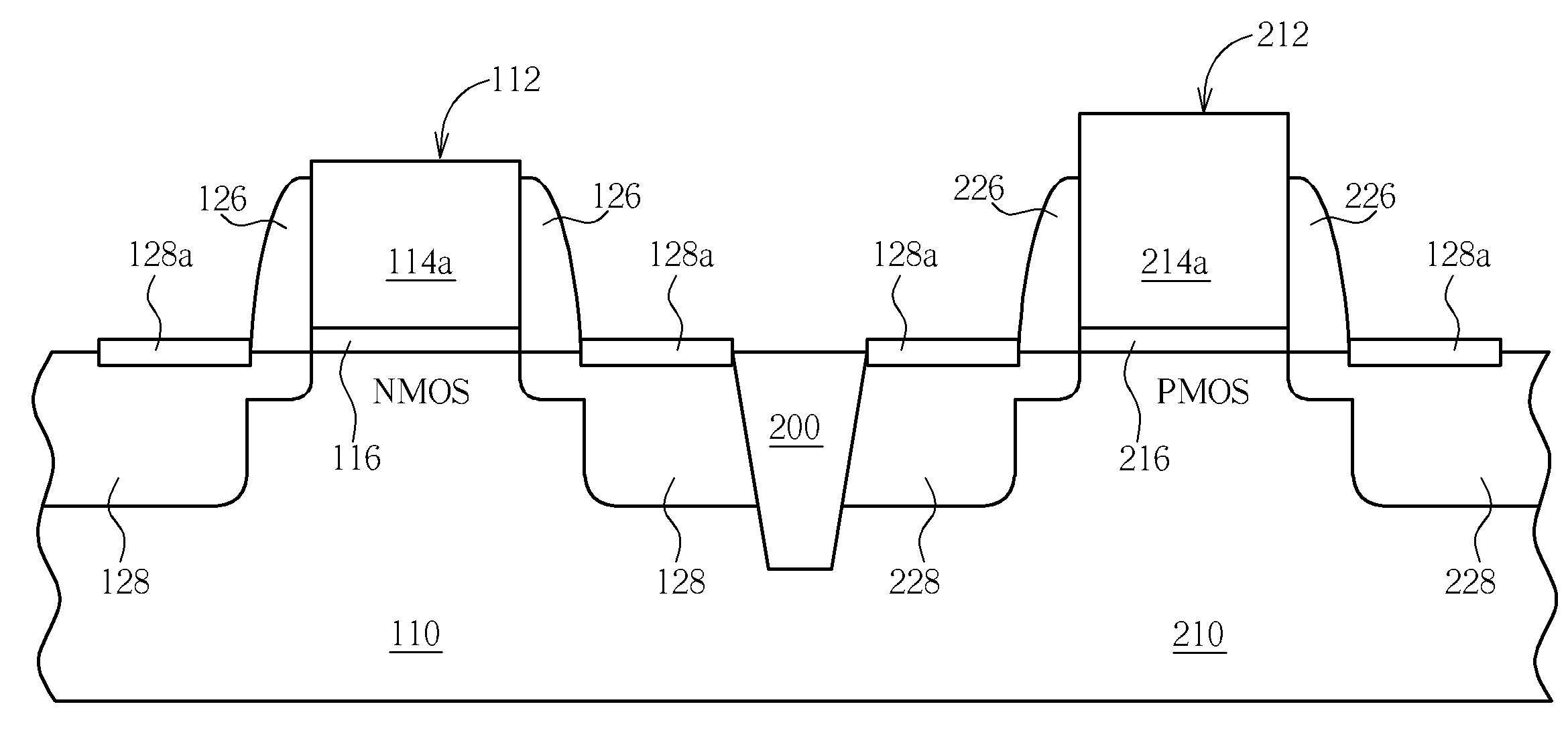
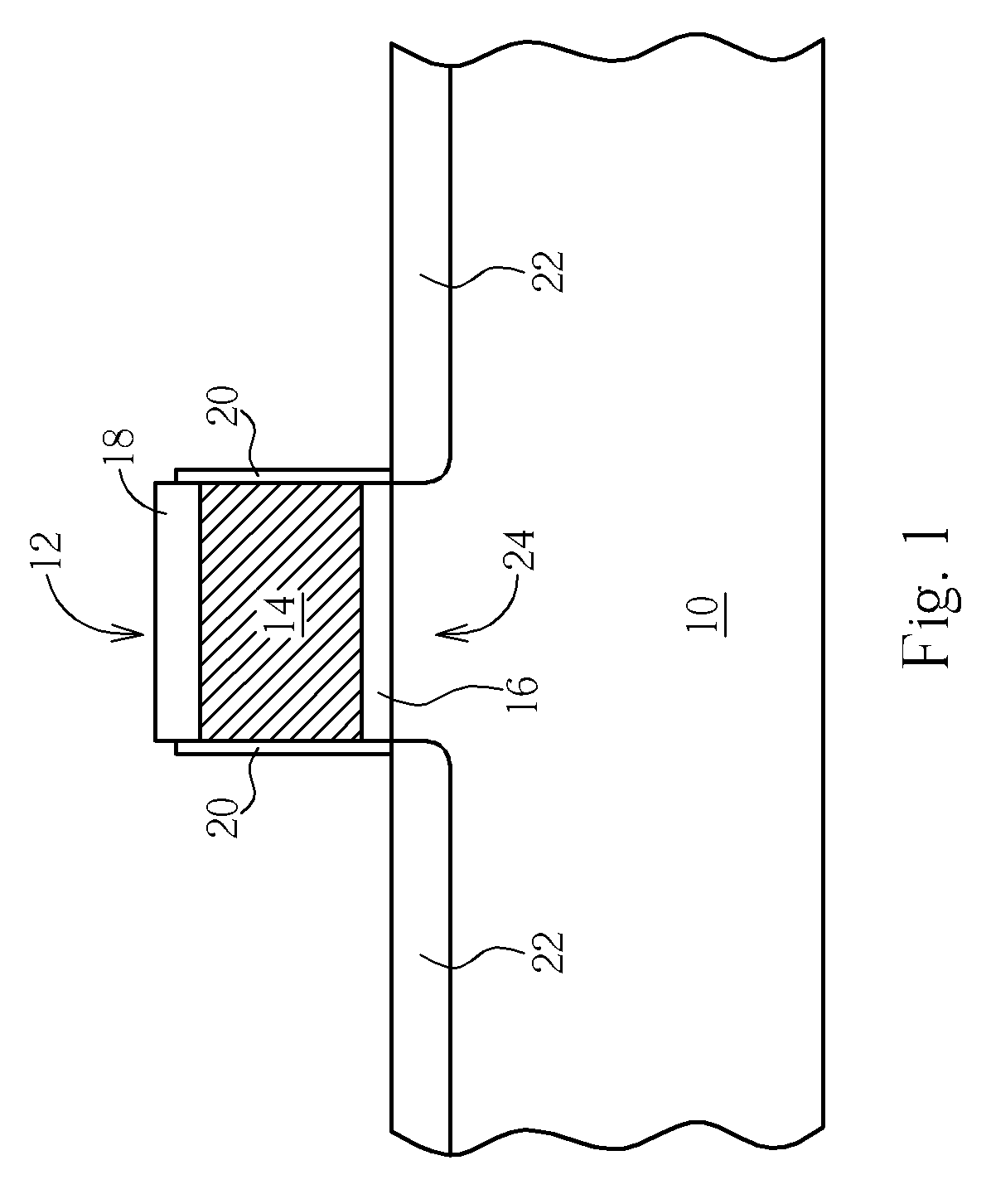
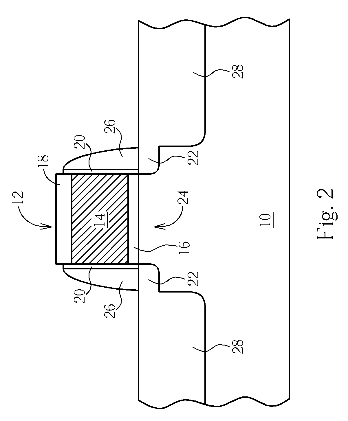
[0025]In describing the preferred embodiments of the present invention, reference will be made herein to FIGS. 1-31 of the drawings. Features of the invention are not drawn to scale in the drawings. It is to be understood that some lithographic, ion implanting and etching processes relating to the present invention method are known in the art and thus not explicitly shown in the drawings.

[0026]Please refer to FIGS. 1-9. FIGS. 1-9 are schematic, cross-sectional diagrams illustrating the method for forming fully silicided gate electrode of a metal-oxide-semiconductor (MOS) transistor device in accordance with one preferred embodiment of this invention. It is noted that this invention is applicable to both NMOS and PMOS processes.

[0027]As shown in FIG. 1, a semiconductor substrate 10 is provided. According to this invention, the semiconductor substrate 10 may be a silicon substrate or a silicon-on-insulator (SOI) substrate, but not limited thereto. Preferably, the semiconductor substra...


PUM


Abstract

A method for forming a fully silicided gate is disclosed. A gate structure of a transistor device is provided on a substrate. A mask layer is spin-on coated over the substrate to cover the gate structure and source / drain regions of the transistor device. The mask layer is etched back to expose a silicon layer of the gate structure. The silicon layer of the gate structure is then fully silicided. The mask layer is then removed from the substrate to expose the source / drain regions. The source / drain regions are finally silicided.

Description

BACKGROUND OF THE INVENTION[0001]1. Field of the Invention[0002]The present invention relates generally to semiconductor processing. More specifically, the present invention relates to a method for forming fully silicided gate electrodes in a semiconductor device.[0003]2. Description of the Prior Art[0004]As semiconductor technology advances, semiconductor devices are becoming increasingly smaller. However, this scaling down of devices may cause problems. For example, as gate oxides are scaled down, gate capacitance due to polysilicon depletion issues becomes more problematic, adversely affecting device performance. Therefore, one solution to this problem is the use of different metal gates for both NMOS and PMOS field effect transistors to serve as a replacement to polysilicon gates. However, the formation and integration of these dual metal gates are complex tasks as compared to form traditional doped polysilicon gates.[0005]Therefore, instead of the formation of dual metal gates,...

Claims


Application Information

Patent Timeline
IPC IPC(8): H01L21/336H01L21/28
CPCH01L21/28097H01L21/7624H01L29/66545H01L29/66507H01L21/823835
Inventor HSU, CHIA-JUNGLIN, CHIN-HSIANGCHENG, LI-WEI
Owner UNITED MICROELECTRONICS CORP
Why Eureka
Try Eureka